LSDEV-WI01-A20 LS Research, LSDEV-WI01-A20 Datasheet - Page 15
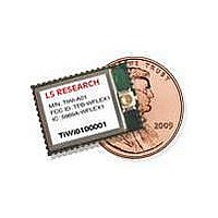
LSDEV-WI01-A20
Manufacturer Part Number
LSDEV-WI01-A20
Description
WiFi / 802.11 Modules & Development Tools TiWi RF Dev Kit
Manufacturer
LS Research
Datasheet
1.450-0009.pdf
(31 pages)
Specifications of LSDEV-WI01-A20
Wireless Frequency
2412 MHz to 2472 MHz
Interface Type
SDIO
Modulation
GFSK, CCK, OFDM
Operating Voltage
3 V to 4.8 V
Output Power
12.5 dBm to 20 dBm
Antenna
U.FL Connector for External Antenna (Not Included)
Operating Temperature Range
- 40 C to + 85 C
Lead Free Status / RoHS Status
Lead free / RoHS Compliant


WLAN POWER-UP SEQUENCE
The information in this document is subject to change without notice.
Confirm the data is current by downloading the latest revision from www.lsr.com.
330-0041-Rev2.4
The following sequence describes device power-up from shutdown. Only the WLAN Core is enabled; the
BT and FM cores are disabled.
The duration of T1 is defined as the time from WL_EN=high until Fref is valid for the SoC, T1 ~55ms
The duration of T2 depends on:
– Operating system
– Host enumeration for the SDIO/WSPI
– PLL configuration
– Firmware download
– Releasing the core from reset
– Firmware initialization
1. No signals are allowed on the IO pins if no IO power supplied, because the IOs are not 'fail
safe’. Exceptions are CLK_REQ_OUT, SLOWCLK, XTALP and AUD_xxx, which are failsafe and
can tolerate external voltages with no VDDS and DC2DC".
2. VBAT,VIO and SLOWCLK must be available before WL_EN.
3. T
A.
wakeup
After this sequence is completed, the device is in the low VIO-leakage state while in shutdown.
= T1 + T2
Figure 4-1: TiWi Power-up Sequence Requirements
Copyright © 2010 LS Research, LLC
TiWi-R1 TRANSCEIVER MODULE
DATASHEET
Page 15 of 31
Related parts for LSDEV-WI01-A20
Image
Part Number
Description
Manufacturer
Datasheet
Request
R

Part Number:
Description:
WiFi / 802.11 Modules & Development Tools Wi-FLEX 802.11 b/g/n Dev Kit
Manufacturer:
LS Research

Part Number:
Description:
DEV KIT, PROFLEX01-R2 F ANTENNA
Manufacturer:
LS Research
Datasheet:
Part Number:
Description:
TIWI5 MODULE, ROHS
Manufacturer:
LS Research
Datasheet:
Part Number:
Description:
TiWi-SL EM with Chip Antenna
Manufacturer:
LS Research
Datasheet:

Part Number:
Description:
WiFi / 802.11 Modules & Development Tools TiWi01-R2 Module with U.FL Connector
Manufacturer:
LS Research
Datasheet:

Part Number:
Description:
Antennas 2.4 GHz Dipole Antenna
Manufacturer:
LS Research
Datasheet:
Part Number:
Description:
Bluetooth / 802.15.1 Modules TiWi-uB2 Module,Tray BT 2.1+ EDR, BLE 4.0
Manufacturer:
LS Research
Datasheet:
Part Number:
Description:
Bluetooth / 802.15.1 Modules TiWi-uB2 Module, TR BT 2.1+ EDR, BLE 4.0
Manufacturer:
LS Research
Datasheet:
Part Number:
Description:
Bluetooth / 802.15.1 Modules TiWi-uB2 Mod,CutTape BT 2.1+ EDR, BLE 4.0
Manufacturer:
LS Research
Datasheet:
Part Number:
Description:
WiFi / 802.11 Modules TiWi5 Module, Reel WLAN + BT 2.1 + EDR
Manufacturer:
LS Research