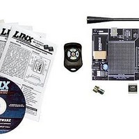
MDEV-418-HH-KF1-MS Linx Technologies Inc, MDEV-418-HH-KF1-MS Datasheet - Page 3
MDEV-418-HH-KF1-MS
Manufacturer Part Number
MDEV-418-HH-KF1-MS
Description
RF Modules & Development Tools 1 Button MS Keyfob Dev Sys 418MHz
Manufacturer
Linx Technologies Inc
Datasheet
1.MDEV-418-HH-KF5-MS.pdf
(7 pages)
Specifications of MDEV-418-HH-KF1-MS
Product
RF Development Tools
Maximum Frequency
418 MHz
Supply Voltage (max)
9 V
Lead Free Status / RoHS Status
Lead free / RoHS Compliant


SETTING THE TRANSMITTER ADDRESS
BUTTON ASSIGNMENTS
Figure 3: OTX-***-HH-KF#-MS Button Assignments
Page 4
The Keyfobs are all supplied from the
factory with a default address and all
buttons authorized. The address is
changed by using a paper clip or probe
to press the CREATE_ADDR button on
the board through the hole in the back
of the case. When the button is
depressed, a LED will light up in the
MODE_IND window, indicating that the
address is being created. The address
will be randomized for as long as the
button is held down. When the button is
released, the randomized address is saved and the LED will begin flashing to
indicate that the Control Permissions may now be set. Press the buttons that the
Keyfob user will have the authority to access. Press the CREATE_ADDR button
with the paper clip again or wait 17 seconds for it to time out. The address and
Control Permissions are now set. The decoder will need to learn the address
before it will accept any transmissions. Please see the Typical Applications
section of this data guide or the MS Series Decoder Data Guide for details.
The Keyfob is available in five unique button configurations. Those
configurations and the corresponding switch numbers are shown in the figure
below. The table shows which encoder data line has been assigned to each
switch. When a button is pressed, the data line will go high, causing the
corresponding data line on the decoder to go high if the addresses match.
S1
S5
S4
S2
S3
S1
S4
S2
S4
S5
S2
S3
Figure 2: CREATE_ADDR Button Access
Button
S1
S2
S3
S4
S5
S4
S5
S2
CREATE_ADDR
Button Access
Data Line
D0
D1
D2
D3
D4
THE DECODER BOARD
Figure 4: The Decoder Board RF Area
The Prototyping Area
The Power Supply
The RF Area
The decoder board included with the evaluation kit uses the LR Series receiver
to receive the signal from the Keyfob transmitter and then feeds it into the MS
Series decoder. The board is designed to allow full access to the many features
of the decoder and to speed development and integration of the LR and MS into
a product. The following sections describe the features of this board in detail.
The prototyping area on the decoder board contains a large area of plated
through-holes so that external circuitry can be placed on the board. This circuitry
can be interfaced with the MS Series decoder through the breakout header to the
right of the holes. At the bottom of this area is a row connected to the 3V power
supply and at the top is a row connected to ground.
All of the data lines are connected to a wire-wrap header to the right, allowing
easy access from the prototyping area. The Decoder Data and TX ID lines are
also available on the header as well as the PDN line from the RF module. This
allows complete control of the entire system from the prototyping area, giving the
designer a great deal of flexibility in using the board.
The power supply on the decoder board consists of a standard 9V battery and
power jack connected to a 3.0V voltage regulator. It can provide approximately
500mA of current to the prototyping area, so if the added circuitry will need more
than this, the designer must add an external supply. If the circuit will consistently
draw more than 100mA of current, it might be better to use the power jack rather
than the battery, as the battery may run down fairly quickly, reducing testing and
development time.
The jack accepts a standard 5.5mm plug with the tip ground and the outer shell
7 to 16VDC positive supply. While a reverse voltage protection diode has been
included on the board to protect the circuitry in case the voltage on the plug is
reversed, it is still a good idea to double-check the polarity.
The figure below shows the RF area of the development board. The board uses
the LR Series receiver as shown. Attach the included antenna to the reverse
polarity SMA connector before operation.
Page 5
Related parts for MDEV-418-HH-KF1-MS
Image
Part Number
Description
Manufacturer
Datasheet
Request
R

Part Number:
Description:
KIT MASTER DEV MS KEYFOB 418MHZ
Manufacturer:
Linx Technologies Inc
Datasheet:

Part Number:
Description:
KIT DEV MS HANDHELD TX 418MHZ
Manufacturer:
Linx Technologies Inc
Datasheet:

Part Number:
Description:
KIT DEV TX 418MHZ HS COMPACT
Manufacturer:
Linx Technologies Inc
Datasheet:

Part Number:
Description:
KIT DEV TX 418MHZ MS SERIES
Manufacturer:
Linx Technologies Inc
Datasheet:

Part Number:
Description:
KIT DEV TX 418MHZ HS LONG-RANGE
Manufacturer:
Linx Technologies Inc
Datasheet:

Part Number:
Description:
RF Modules & Development Tools 3 Button MS Keyfob Dev Sys 418MHz
Manufacturer:
Linx Technologies Inc
Datasheet:
Part Number:
Description:
RF Modules & Development Tools 4 Button MS Keyfob Dev Sys 418MHz
Manufacturer:
Linx Technologies Inc
Datasheet:
Part Number:
Description:
RF Modules & Development Tools 2 Button MS Keyfob Dev Sys 418MHz
Manufacturer:
Linx Technologies Inc
Datasheet:

Part Number:
Description:
RF Development Tools 1-5 Button Keyfob Dev Sys 418MHz
Manufacturer:
Linx Technologies
Datasheet:

Part Number:
Description:
HOLDER BATTERY 20MM COIN CR2032
Manufacturer:
Linx Technologies Inc
Datasheet:

Part Number:
Description:
MODULE USB LOW SPEED
Manufacturer:
Linx Technologies Inc
Datasheet:

Part Number:
Description:
IC TRANSCODER MT BI-DIR 20-SSOP
Manufacturer:
Linx Technologies Inc
Datasheet:

Part Number:
Description:
IC ENCODER LOW SECURITY 8DIP
Manufacturer:
Linx Technologies Inc
Datasheet:

Part Number:
Description:
IC DECODER MS SERIES 20-SSOP
Manufacturer:
Linx Technologies Inc
Datasheet:
Part Number:
Description:
IC ENCODER MS SERIES 20-SSOP
Manufacturer:
Linx Technologies Inc
Datasheet: