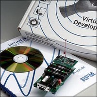
DR7000-EV RFM, DR7000-EV Datasheet - Page 5

DR7000-EV
Manufacturer Part Number
DR7000-EV
Description
RF Modules & Development Tools 3G Transceiver Eval Module 433.92 MHz
Manufacturer
RFM
Datasheet
1.DR7000-EV.pdf
(8 pages)
Specifications of DR7000-EV
Lead Free Status / RoHS Status
Lead free / RoHS Compliant
Current Consumption Monitor (J5)
The current consumption of the TR7000 device may be monitored by removing J5 and connecting an ammeter across the terminals. When
J5 is removed it isolates the TR7000 from VCC powering the on-board processor to give a true reading of the current consumption of only
the TR7000 without the additional current usage of the processor. J5 must be installed to power the TR7000 if not using the header for current
measurement.
Theory of Operation
The DR7000-EV evaluation module is centered around the TR7000 ASH Transceiver. The DR7000-EV may operate in
backward compatible 2G mode, or in the enhanced 3G mode. Since 3G mode requires the use of a serial I/O port to configure
internal registers, the module includes an on-board Silicon Labs C8051F330 microcontroller to control access to the serial
port. When 2G mode is enabled the microcontroller serves no function. When 3G mode is enabled the microcontroller
constantly scans pins 8-15 for a change of logic state. When a state change is detected on one or more of these pins, the
microcontroller automatically updates the internal configuration registers via the serial port of the TR7000. The microcontroller
assumes full control of the CFG pin, CFGCLK pin, and CFGDAT pin in 3G mode to continuously update the internal registers.
The DR7000-EV module is designed to demonstrate the performance of the TR7000 ASH Transceiver at 4.8kbps, although
other data rates are possible with changes in on-board component values. See pin descriptions and refer to the TR7000
datasheet.
The DR7000-EV module may be mounted on a prototype assembly using standard 0.1” spacing, 10-pin headers spaced 0.9”
apart.
2G Mode Operation
The DR7000-EV may operate in 2G mode. See pin 15 description and Power-up Mode Select (J2) section for mode select
details. In 2G mode, the CFGCLK pin (18) and CFGDAT pin (17) operate as CTRL0 and CTRL1, respectively, just as for
second-generation devices. The CFGCLK and CFGDAT pins are a high impedance input allowing external control for 2G
configuration. The logic levels on CFGCLK (CTRL0) and CFGDAT (CTRL1) control the default 2G operation as shown
below:
433.92 MHz
RF Monolithics, Inc.
RFM Europe
©1999 by RF Monolithics, Inc. The stylized RFM logo are registered trademarks of RF Monolithics, Inc.
Phone: (972) 233-2903
Phone: 44 1963 251383
CFGCLK (CNTRL0)
0
1
0
1
Transceiver Module
Fax: (972) 387-8148
Fax: 44 1963 251510
CFGDAT (CNTRL1)
0
0
1
1
TX OOK
TX ASK
SLEEP
MODE
RX
J5 Header
E-mail: info@rfm.com
http://www.rfm.com
DR7000EV-071107
J2 Header
Page 5 of 8


