C8051F015DK Silicon Laboratories Inc, C8051F015DK Datasheet - Page 108
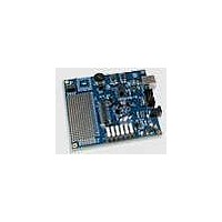
C8051F015DK
Manufacturer Part Number
C8051F015DK
Description
MCU, MPU & DSP Development Tools Dev Kit for F015-19
Manufacturer
Silicon Laboratories Inc
Datasheet
1.C8051F005-TB.pdf
(171 pages)
Specifications of C8051F015DK
Processor To Be Evaluated
C8051F01x
Interface Type
USB
Lead Free Status / RoHS Status
Lead free / RoHS Compliant


WEAKPUD
Bit7:
Bit6:
Bits5-1: UNUSED. Read = 00000b, Write = don’t care.
Bit0:
Example Usage of XBR0, XBR1, XBR2:
When selected, the digital resources fill the Port I/O pins in order (top to bottom as shown in
Table 15.1) starting with P0.0 through P0.7, and then P1.0 through P1.7, and finally P2.0
through P2.7. If the digital resources are not mapped to the Port I/O pins, they default to their
matching internal Port Register bits.
Example1: If XBR0 = 0x11, XBR1 = 0x00, and XBR2 = 0x40:
P0.0=SDA, P0.1=SCL, P0.2=CEX0, P0.3=CEX1, P0.4 … P2.7 map to corresponding Port I/O.
Example2: If XBR0 = 0x80, XBR1 = 0x04, and XBR2 = 0x41:
P0.0=CP0, P0.1=/INT0, P0.2 = CNVSTR, P0.3 … P2.7 map to corresponding Port I/O.
R/W
Bit7
0: Weak Pull-ups Enabled (except for Ports whose I/O are configured as push-pull)
1: Weak Pull-ups Disabled
0: Crossbar Disabled
1: Crossbar Enabled
CNVSTE: ADC Convert Start Input Enable Bit
0: CNVSTR unavailable at Port pin.
1: CNVSTR routed to Port Pin.
WEAKPUD: Port I/O Weak Pull-up Disable Bit
XBARE: Crossbar Enable Bit
XBARE
R/W
Bit6
Figure 15.5. XBR2: Port I/O CrossBar Register 2
R/W
Bit5
-
R/W
Bit4
-
Rev. 1.7
R/W
Bit3
-
R/W
Bit2
-
C8051F000/1/2/5/6/7
C8051F010/1/2/5/6/7
R/W
Bit1
-
CNVSTE
R/W
Bit0
SFR Address:
Reset Value
00000000
0xE3
108
Related parts for C8051F015DK
Image
Part Number
Description
Manufacturer
Datasheet
Request
R

Part Number:
Description:
SMD/C°/SINGLE-ENDED OUTPUT SILICON OSCILLATOR
Manufacturer:
Silicon Laboratories Inc
Part Number:
Description:
Manufacturer:
Silicon Laboratories Inc
Datasheet:
Part Number:
Description:
N/A N/A/SI4010 AES KEYFOB DEMO WITH LCD RX
Manufacturer:
Silicon Laboratories Inc
Datasheet:
Part Number:
Description:
N/A N/A/SI4010 SIMPLIFIED KEY FOB DEMO WITH LED RX
Manufacturer:
Silicon Laboratories Inc
Datasheet:
Part Number:
Description:
N/A/-40 TO 85 OC/EZLINK MODULE; F930/4432 HIGH BAND (REV E/B1)
Manufacturer:
Silicon Laboratories Inc
Part Number:
Description:
EZLink Module; F930/4432 Low Band (rev e/B1)
Manufacturer:
Silicon Laboratories Inc
Part Number:
Description:
I°/4460 10 DBM RADIO TEST CARD 434 MHZ
Manufacturer:
Silicon Laboratories Inc
Part Number:
Description:
I°/4461 14 DBM RADIO TEST CARD 868 MHZ
Manufacturer:
Silicon Laboratories Inc
Part Number:
Description:
I°/4463 20 DBM RFSWITCH RADIO TEST CARD 460 MHZ
Manufacturer:
Silicon Laboratories Inc
Part Number:
Description:
I°/4463 20 DBM RADIO TEST CARD 868 MHZ
Manufacturer:
Silicon Laboratories Inc
Part Number:
Description:
I°/4463 27 DBM RADIO TEST CARD 868 MHZ
Manufacturer:
Silicon Laboratories Inc
Part Number:
Description:
I°/4463 SKYWORKS 30 DBM RADIO TEST CARD 915 MHZ
Manufacturer:
Silicon Laboratories Inc
Part Number:
Description:
N/A N/A/-40 TO 85 OC/4463 RFMD 30 DBM RADIO TEST CARD 915 MHZ
Manufacturer:
Silicon Laboratories Inc
Part Number:
Description:
I°/4463 20 DBM RADIO TEST CARD 169 MHZ
Manufacturer:
Silicon Laboratories Inc