MCT2 Vishay, MCT2 Datasheet - Page 2
MCT2
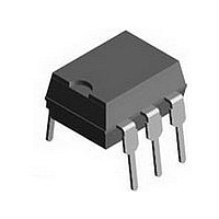
Manufacturer Part Number
MCT2
Description
Transistor Output Optocouplers Phototransistor Out
Manufacturer
Vishay
Datasheet
1.MCT2.pdf
(10 pages)
Specifications of MCT2
Maximum Input Diode Current
60 mA
Maximum Reverse Diode Voltage
6 V
Output Device
Phototransistor
Output Type
DC
Configuration
1 Channel
Input Type
DC
Maximum Collector Emitter Voltage
30 V
Isolation Voltage
5300 Vrms
Current Transfer Ratio
60 %
Maximum Forward Diode Voltage
1.5 V
Maximum Collector Current
100 mA
Maximum Power Dissipation
150 mW
Maximum Operating Temperature
+ 100 C
Minimum Operating Temperature
- 55 C
Package / Case
PDIP-6
Number Of Elements
1
Reverse Breakdown Voltage
6V
Forward Voltage
1.5V
Forward Current
60mA
Collector-emitter Voltage
30V
Package Type
PDIP
Collector Current (dc) (max)
100mA
Power Dissipation
150mW
Pin Count
6
Mounting
Through Hole
Operating Temp Range
-55C to 100C
Operating Temperature Classification
Industrial
Lead Free Status / RoHS Status
Lead free / RoHS Compliant
Available stocks
Company
Part Number
Manufacturer
Quantity
Price

Part Number:
MCT2
Manufacturer:
FAIRCHILD/仙童
Quantity:
20 000
Company:
Part Number:
MCT210
Manufacturer:
FAIRCHIL
Quantity:
162
Part Number:
MCT210
Manufacturer:
FAIRCHILD/仙童
Quantity:
20 000
Part Number:
MCT210SD
Manufacturer:
FAIRCHILD/仙童
Quantity:
20 000
Part Number:
MCT2200
Manufacturer:
FAIRCHILD/仙童
Quantity:
20 000
Part Number:
MCT2201
Manufacturer:
FAIRCHILD/仙童
Quantity:
20 000


MCT2/ MCT2E
Vishay Semiconductors
Absolute Maximum Ratings
T
Stresses in excess of the absolute Maximum Ratings can cause permanent damage to the device. Functional operation of the device is
not implied at these or any other conditions in excess of those given in the operational sections of this document. Exposure to absolute
Maximum Rating for extended periods of the time can adversely affect reliability.
Input
Output
Coupler
www.vishay.com
2
Reverse voltage
Forward current
Surge current
Power dissipation
Collector-emitter breakdown
Emitter-base breakdown
voltage
Collector current
Power dissipation
Isolation test voltage
Creepage
Clearance
Isolation thickness between
emitter and detector
Comparative tracking index per
DIN IEC 112/VDE0303,part 1
Isolation resistance
Storage temperature
Operating temperature
Junction temperature
Soldering temperature
amb
= 25 °C, unless otherwise specified
Parameter
Parameter
Parameter
t ≤ 10 µs
t < 1.0 ms
V
V
max. 10 s dip soldering:
distance to seating plane
≥ 1.5 mm
IO
IO
= 500 V, T
= 500 V, T
Test condition
Test condition
Test condition
amb
amb
= 25 °C
= 100 °C
Symbol
Symbol
Symbol
BV
V
P
P
I
V
T
T
R
R
T
FSM
V
CEO
I
I
T
I
diss
diss
ISO
EBO
stg
stg
sld
F
C
C
IO
IO
R
j
- 55 to + 150
- 55 to + 100
Value
Value
Value
5300
≥ 7.0
≥ 7.0
≥ 0.4
10
10
100
100
150
175
100
260
6.0
2.5
7.0
60
70
50
12
11
Document Number 83731
Rev. 1.4, 26-Oct-04
V
Unit
mW
Unit
mW
Unit
mm
mm
mm
mA
mA
mA
°C
°C
°C
°C
RMS
Ω
Ω
V
A
V
V
Related parts for MCT2
Image
Part Number
Description
Manufacturer
Datasheet
Request
R

Part Number:
Description:
357-036-542-201 CARDEDGE 36POS DL .156 BLK LOPRO
Manufacturer:
Vishay
Datasheet:
Part Number:
Description:
357-036-542-201 CARDEDGE 36POS DL .156 BLK LOPRO
Manufacturer:
Vishay
Datasheet:
Part Number:
Description:
357-036-542-201 CARDEDGE 36POS DL .156 BLK LOPRO
Manufacturer:
Vishay
Datasheet:
Part Number:
Description:
357-036-542-201 CARDEDGE 36POS DL .156 BLK LOPRO
Manufacturer:
Vishay
Datasheet:
Part Number:
Description:
357-036-542-201 CARDEDGE 36POS DL .156 BLK LOPRO
Manufacturer:
Vishay
Datasheet: