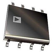
IR1153SPBF International Rectifier, IR1153SPBF Datasheet - Page 8

IR1153SPBF
Manufacturer Part Number
IR1153SPBF
Description
IC PFC ONE CYCLE CONTROL 8SOIC
Manufacturer
International Rectifier
Datasheet
1.IR1153STRPBF.pdf
(20 pages)
Specifications of IR1153SPBF
Mode
Continuous Conduction (CCM)
Frequency - Switching
18.3kHz ~ 25kHz
Current - Startup
26µA
Voltage - Supply
14 V ~ 17 V
Operating Temperature
-25°C ~ 125°C
Mounting Type
*
Package / Case
*
Startup Current
26µA
Operating Supply Current
7mA
Duty Cycle (%)
99%
Frequency
22.2kHz
Digital Ic Case Style
SOIC
No. Of Pins
8
Operating Temperature Range
-25°C To +125°C
Peak Reflow Compatible (260 C)
Yes
Rohs Compliant
Yes
Supply Voltage Range
14V To 17V
Package
8-lead SOIC
Circuit
PFC IC
Vcc Range (v)
14V-17V
Out Peak Current (a)
+/- 0.75
Switching Frequency (khz)
22.2
Environment
Industrial
Over-voltage Protection
Yes
Brown-out Protection
Yes
Pbf
Yes
Lead Free Status / RoHS Status
Lead free / RoHS Compliant
www.irf.com
The μPFC IR1153 IC is intended for power factor
correction in continuous conduction mode Boost PFC
converters operating at fixed switching frequency with
average current mode control. The IC operates based
on IR's proprietary "One Cycle Control" (OCC) PFC
algorithm based on the concept of resettable
integrator.
Theory of Operation
The OCC algorithm based on the resettable integrator
concept works using two loops - a slow outer voltage
loop and a fast inner current loop. The outer voltage
loop monitors the VFB pin and generates an error
signal which controls the amplitude of the input current
admitted into the PFC converter. In this way, the outer
voltage loop maintains output voltage regulation. The
voltage loop bandwidth is kept low enough to not track
the 2xf
generates an almost DC error signal under steady
state conditions.
The inner current loop maintains the sinusoidal profile
of the input current and thus is responsible for power
factor correction. The information about the sinusoidal
variation in input voltage is inherently available in the
input line current (or boost inductor current). Thus
there is no need to sense the input voltage to
generate a current reference. The current loop
employs the boost inductor current information to
generate PWM signals with a proportional sinusoidal
variation. This controls the shape of the input current
to be proportional to and in phase with the input
voltage. Average current mode operation is envisaged
by filtering the switching frequency ripple from the
current sense signal using an appropriately sized on-
chip RC filter. This filter also contributes to the
bandwidth of the current control loop. Thus the filter
bandwidth has to be high enough to track the 120Hz
rectified, sinusoidal current waveform and also filter
out the switching frequency ripple in the inductor
current. In IR1153 this averaging function can
effectively filter high ripple current ratios (as high as
40% at maximum input current) to accommodate
designs with small boost inductances.
The IC determines the boost converter instantaneous
duty cycle based on the resettable integrator concept.
The required signals are the voltage feedback loop
error signal V
DC offset of V
V
cycle, saw-tooth signal called the PWM Ramp which
has an amplitude V
V
IR1153 General Description
ISNS
m*
f
SW
. The resettable integrator generates a cycle-by-
.
AC
ripple in the output voltage and thus
m
COMP,START
(which is the V
m
and period 1/f
) and the current sense signal
COMP
pin voltage minus a
SW
hence a slope of
8
The current sense signal is amplified by the current
amplifier by a factor g
node where it is subtracted from V
summer voltage (= V
voltage is compared with the PWM ramp by the
PWM comparator of the IC to determine the gate
drive duty cycle. The instantaneous duty is
mathematically given by:
D = (V
Assuming steady state condition where the voltage
feedback loop is well regulated (V
signals) & hence instantaneous duty cycle follows
the boost-converter equation (D = 1 – V
the control equation can be re-written as:
V
Further, recognizing that V
arranging yields:
g
Since V
I
Thus the inductor current follows the input voltage
waveform & by definition power factor correction is
achieved.
Feature set
Fixed Frequency Operation
The IC is programmed to operate at a fixed
frequency of 22.2kHz (Typ). Internalization of the
oscillator offers excellent noise immunity even in
the noisy PFC environment while integration of the
oscillator into the OCC core of the IC eliminates
need for digital calibration circuits. Both these
factors render the gate drive jitter free thus
contributing to elimination of audible noise in PFC
magnetics.
IC Supply Circuit & Low start-up current
The IR1153 UVLO circuit maintains the IC in UVLO
mode during start-up if VCC pin voltage is less than
the VCC turn-on threshold, V
consumption is less than 75uA. Should VCC pin
voltage should drop below V
operation, the IC is pushed back into UVLO mode
and VCC pin has to exceed V
operation. There is no internal voltage clamping of
the VCC pin.
User initiated Micropower Sleep mode
The IC can be actively pushed into a micropower
Sleep Mode where current consumption is less
than 75uA by pulling OVP/EN pin below the Sleep
threshold, V
This allows the user to disable PFC during
application stand-by situations in order to meet
stand-by regulations. Since V
even logic level signals can be employed.
L
DC
(t) α V
m
= g
.I
L
(t).R
m
DC
IN
m
- g
.V
, V
(t)
SNS
ISNS
DC
OUT
SLEEP
.V
= V
/(V
ISNS
& g
m
IN
even while VCC is above V
V
)/V
(t)/V
DC
IN
(t)/V
m
are constant terms:
DC
OUT
m
–g
and fed into the summing
OUT
)
DC
ISNS
© 2011 International Rectifier
*V
CC,ON
CC,UVLO
SLEEP
ISNS
= I
CC,ON
IR1153S
m
m
L
). The summer
again for normal
is less than 1V,
(t).R
to generate the
& V
during normal
and current
SNS
OUT
IN
(t)/V
and re-
are DC
CC,ON
OUT
),
.


