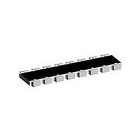
CRA12E10110K0JTR Vishay, CRA12E10110K0JTR Datasheet

Resistor Networks & Arrays 10Term 10Kohms 5% Convex/Scalloped

CRA12E10110K0JTR

Manufacturer Part Number
CRA12E10110K0JTR
Description
Resistor Networks & Arrays 10Term 10Kohms 5% Convex/Scalloped
Manufacturer
Vishay
Type
Arrayr
Series
CRA12E, CRA12Sr
Datasheet

Specifications of CRA12E10110K0JTR

Technology
Thick Film
Resistance
10kohm
Power Rating Per Resistor
1/10W
Number Of Resistors
9
Tolerance (+ Or -)
5%
Circuit Designator
BUS
Mounting Style
Surface Mount
Temperature Coefficient
±200
Military Standard
Not Required
Operating Temp Range
-55C to 155C
No. Of Terminals
10
Case Style
Molded
Failure Rate
Not Required
Termination Style
Convex
Terminal Pitch
1.27
Product Length (mm)
6.4mm
Product Depth (mm)
3.05mm
Product Height (mm)
0.55mm
Product Type
Arrays
Circuit Type
Isolated
Resistor Values
10 KOhms
Tolerance
5 %
Power Rating
0.5 Watt (1/2 Watt)
Number Of Pins
10
Operating Temperature Range
- 55 C to + 150 C
Dimensions
3.05 mm W x 6.4 mm L x 0.55 mm H
Voltage Rating
50 Volts
Lead Free Status / RoHS Status
Compliant

Available stocks

Company
Part Number
Manufacturer
Quantity
Price
Part Number:
CRA12E10110K0JTR
Manufacturer:
VISHAY
Quantity:
40 000
CRA12E, CRA12S
Vishay
Note
(1)
Note
(2)
www.vishay.com
248
STANDARD ELECTRICAL SPECIFICATIONS
MODEL
CRA12E
CRA12S
TECHNICAL SPECIFICATIONS
PARAMETER
Rated dissipation at P
Limiting element voltage
U
Insulation voltage U
Insulation resistance
Category temperature range
PART NUMBER AND PRODUCT DESPRIPTION
Part Number: CRA12E08347K0JTR
Product Description: CRA12E 08 03 47K 5 % RB8 e3
CRA12E
CRA12E
CRA12S
MODEL
CRA12
MODEL
Power rating depends on the max. temperature at the solder point, the component placement density and the substrate material.
Preferred way for ordering products is by use of the PART NUMBER.
max.
AC/DC
C
TERMINAL STYLE
01; 02; 20
CIRCUIT
R
03
PIN
ins
08
08
10
70
S
E
(1 min)
A
(1)
POWER RATING
Zero-Ohm-Resistor: R
1
P
0.100
0.125
70 °C
CIRCUIT
W
2
PIN
(2)
08
10
03
01
02
03
20
W per element
For technical questions, contact:
Thick Film Resistor Array
E
UNIT
CIRCUIT
°C
Ω
V
V
1 = 01
2 = 02
3 = 03
8 = 20
LIMITING ELEMENT
VOLTAGE MAX.
0
max.
RESISTANCE VALUE
= 50 mΩ, I
0R0 = Jumper
V≅
50
8
47K = 47 kΩ
10R = 10 Ω
1M = 1 MΩ
0000 = 0 Ω Jumper
K = Thousand
47K
R = Decimal
M = Million
3
VALUE
CRA12E AND CRA12S
max.
CIRCUIT 01; 02; 20
= 1.5 A
4
TEMPERATURE
thickfilmchip@vishay.com
FEATURES
• Convex terminal array available with either
• Wide ohmic range: 10R to 1M0
• 8 or 10 terminal package with isolated resistors
• Pure tin solder contacts on Ni barrier layer,
• Compliant to RoHS Directive 2002/95/EC
• Halogen-free according to IEC 61249-2-21 definition
COEFFICIENT
scalloped corners (E version) or square corners
(S version)
provides compatibility with lead (Pb)-free and lead
containing soldering processes
0.1
ppm/K
± 100
± 200
7
TOLERANCE
Z = 0 Ω Jumper
TOLERANCE
K
G = ± 2 %
± 1 %
± 2 %
± 5 %
F = ± 1 %
J = ± 5 %
5 %
- 55 to + 155
TOLERANCE
0
± 2; ± 5
> 10
100
50
± 1
%
J
9
PACKAGING
PACKAGING
RB8
RB8
RD7
T
CRA12E AND CRA12S
RESISTANCE
TR
TL
10R to 1M0
RANGE
CIRCUIT 03
R
Document Number: 31003
Ω
0.125
Revision: 10-Dec-10
LEAD (Pb)-FREE
termination finish
e3 = Pure tin
Up to 2 digits
SPECIAL
e3
E24; E96
SERIES
E24

Related parts for CRA12E10110K0JTR

CRA12E10110K0JTR Summary of contents

Page 1

... CIRCUIT VALUE Decimal Thousand Million 0000 = 0 Ω Jumper 47K RESISTANCE VALUE 10R = 10 Ω 47K = 47 kΩ MΩ 0R0 = Jumper For technical questions, contact: thickfilmchip@vishay.com RESISTANCE TOLERANCE RANGE % Ω ± 1 10R to 1M0 ± 2; ± 5 CRA12E AND CRA12S CIRCUIT 03 0.125 50 100 9 > 155 ...

Page 2

... For technical questions, contact: thickfilmchip@vishay.com CRA12E, CRA12S TEMPERATURE TOLERANCE COEFFICIENT ± 100 ppm/K ± ± ± ± 200 ppm/K BLISTER TAPE ACC. IEC 60286-3, TYPE II PART NUMBER PRODUCT DESCRIPTION TR RB8 TL RD7 02 Circuit 10 pin Pin 1 20 Circuit Pin 1 www.vishay.com Vishay 249 ...

Page 3

... Ambient Temperature in ° 0.38 1.27 0.55 3.05 WAVE 0.38 1.27 0.55 3.05 REFLOW 0.38 1.27 0.55 3.05 For technical questions, contact: thickfilmchip@vishay.com 125 155 175 E-Version PIN SOLDER PAD DIMENSIONS in millimeters 2.2 4.3 0.57 1.27 0.71 2.2 3.9 0.57 1.27 ...

Page 4

... R + 0.05 Ω) ± (0 0.05 Ω) No burning after 30 s ± 0.05 Ω) ± 0.05 Ω) ± 0.1 Ω) ± 0.05 Ω) No visible damage Marking legible, no visible damage ± (0. 0.05 Ω) ± (0 0.05 Ω) ± 0.05 Ω) max. ± 0.05 Ω) max. www.vishay.com Vishay 251 ...

Page 5

... Vishay disclaims any and all liability arising out of the use or application of any product described herein or of any information provided herein to the maximum extent permitted by law. The product specifications do not expand or otherwise modify Vishay’ ...

Related keywords