HFBR-7924 Avago Technologies US Inc., HFBR-7924 Datasheet - Page 12
HFBR-7924
Manufacturer Part Number
HFBR-7924
Description
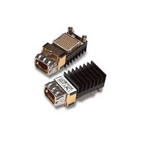
Fiber Optic Transmitters, Receivers, Transceivers 4+4 2.7Gbps Pluggabl e Txcvr Module
Manufacturer
Avago Technologies US Inc.
Datasheet
1.HFBR-7924.pdf
(18 pages)
Specifications of HFBR-7924
Function
Pluggable Transceiver, for Parallel Optics
Product
Transceiver
Wavelength
850 nm
Maximum Rise Time
150 ps
Maximum Fall Time
150 ps
Pulse Width Distortion
0.045 ns
Maximum Output Current
25 mA
Operating Supply Voltage
3.135 V to 3.465 V
Maximum Operating Temperature
+ 80 C
Minimum Operating Temperature
0 C
Optical Fiber Type
TX/RX
Data Transfer Rate
2700MBd
Optical Rise Time
0.15ns
Optical Fall Time
0.15ns
Jitter
0.045ns
Operating Temperature Classification
Commercial
Peak Wavelength
850/860nm
Operating Supply Voltage (min)
3.135V
Operating Supply Voltage (typ)
3.3V
Operating Supply Voltage (max)
3.465V
Output Current
25mA
Operating Temp Range
0C to 80C
Mounting
Screw
Pin Count
100
For Use With
Multimode Glass
Lead Free Status / RoHS Status
Lead free / RoHS Compliant


Table 2. Transceiver Module Pad Description
12
Din Ch 0 - 3 +/- through
Din Ch 0 - 3 +/-
Dout Ch 0 - 3 +/- through
Dout Ch 0 - 3 +/-
DNC
Module Case
Symbol
TX_DIS
TX_EN
TX_FAULT*
TX_RESET*
V
V
SD
V
V
V
V
noise from the power supply, it is recommended to keep the power supplies separate and to use the recommended power supply filtering network
on V
EE
CC
EE
CC
CC
CC
_TX
_RX
_TX
A_RX
B_RX
A_RX and V
CC
A_RX (see Figure 8).
CC
B_RX can be connected to the same power supply. However, to insure maximum receiver sensitivity and minimize the impact of
Functional Description
Receiver differential data outputs for channels 0 through 3: Data outputs are CML compatible. Data
Receiver Signal Detect: LVCMOS Output. Receiver status output indicating valid signal in all
Do NOT Connect. Do not connect to any electrical potential.
Receiver signal common. All receiver voltages are referenced to this potential unless otherwise
Pin preamplifier power supply rail.
Receiver quantizer power supply rail.
Transmitter differential data inputs for channels 0 through 3: Data inputs are CML compatible.
Transmitter Disable: LVCMOS Input (Internal pull down). Control input used to turn off the transmitter
optical outputs. High Active. VCSEL array is off when High. Normal operation is enabled when Low.
Transmitter Enable: LVCMOS Input (Internal pull up). Control input used to enable the transmitter
optical outputs. High Active. VCSEL array is off when Low. Normal operation is enabled when High.
Transmitter Fault: LVCMOS Output. Transmitter status output indicating an eye-safety over-current
condition for any VCSEL, an out of temperature range condition and/or a calibration data corruption
detection. High output state indicates normal operation. Low output state indicates the fault
condition. An asserted FAULT* condition disables the VCSEL array and is cleared by TX_RESET*.
Transmitter Reset: LVCMOS Input (Internal pull up). Control input used to reset the transmitter logic
functions. Active Low. VCSEL array is off when Low. Normal operation is enabled when High.
Transmitter signal common. All transmitter voltages are referenced to this potential unless otherwise
stated. Directly connect these pads to the PC board transmitter ground plane.
Transmitter power supply.
outputs are squelched for de-asserted Signal Detect.
channels. High output state (asserted) indicates valid optical inputs to each and every channel. Low
output state (de-asserted) indicates loss of signal at any of the monitored receiver inputs. All
channels are monitored.
stated. Directly connect these pads to the PC board receiver ground plane.
Transceiver Case Common. Transceiver Case Common incorporates all exposed conductive surfaces
and is electrically isolated from Transmitter Signal Common and Receiver Signal Common.
Related parts for HFBR-7924
Image
Part Number
Description
Manufacturer
Datasheet
Request
R

Part Number:
Description:
RECEIVER FIBER OPTIC 600NM 5MBD
Manufacturer:
Avago Technologies US Inc.
Datasheet:

Part Number:
Description:
RECEIVER FIBER OPTIC 600NM 40KBD
Manufacturer:
Avago Technologies US Inc.
Datasheet:

Part Number:
Description:
RCVR FIBER OPTIC INTERBUS-S
Manufacturer:
Avago Technologies US Inc.
Datasheet:

Part Number:
Description:
RCVR OPT HI PERF VERS LINK HORZ
Manufacturer:
Avago Technologies US Inc.
Datasheet:
Part Number:
Description:
RCVR OPT HI PERF VERS LINK HORZ
Manufacturer:
Avago Technologies US Inc.
Datasheet:

Part Number:
Description:
XMITTER FIBER OPTIC 600NM 5MBD
Manufacturer:
Avago Technologies US Inc.
Datasheet:

Part Number:
Description:
XMITTER FIBER OPTIC 600NM 40KBD
Manufacturer:
Avago Technologies US Inc.
Datasheet:

Part Number:
Description:
XMITTER FIBER OPTIC HIGH PWR ST
Manufacturer:
Avago Technologies US Inc.
Datasheet:
Part Number:
Description:
XMITTER VERSATILE LINK HORZ
Manufacturer:
Avago Technologies US Inc.
Datasheet:
Part Number:
Description:
XMITTER VERSATILE LINK HORZ
Manufacturer:
Avago Technologies US Inc.
Datasheet:

Part Number:
Description:
XMITTER OPT HI PERFORMANCE VERT
Manufacturer:
Avago Technologies US Inc.
Datasheet:

Part Number:
Description:
Fiber Optic Transmitters, Receivers, Transceivers Versatile Link Horiz
Manufacturer:
Avago Technologies US Inc.
Datasheet:
Part Number:
Description:
Fiber Optic Transmitters, Receivers, Transceivers Versatile Link Horiz
Manufacturer:
Avago Technologies US Inc.
Datasheet:
Part Number:
Description:
Fiber Optic Transmitters, Receivers, Transceivers Versatile Link Horiz
Manufacturer:
Avago Technologies US Inc.
Datasheet:

Part Number:
Description:
FIBER OPTIC TRANSMITTER 660NM
Manufacturer:
Avago Technologies US Inc.
Datasheet: