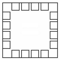
LDS8846003T2 Leadis Technology, LDS8846003T2 Datasheet - Page 5

LDS8846003T2
Manufacturer Part Number
LDS8846003T2
Description
LED Drivers 4Ch no Chrg Pump,4x4 comp to RT9360,SC604
Manufacturer
Leadis Technology
Datasheet
1.LDS8846003T2.pdf
(12 pages)
Specifications of LDS8846003T2
Number Of Segments
4
Operating Supply Voltage
2.7 V to 5.5 V
Maximum Operating Temperature
+ 85 C
Mounting Style
SMD/SMT
Package / Case
TQFN EP
Minimum Operating Temperature
- 40 C
Lead Free Status / RoHS Status
Lead free / RoHS Compliant
LDS8846
PIN DESCRIPTION
PIN FUNCTION
EN is a Device Enable. This pin is high impedance.
There should be a pull down resistor <100k when
control signal is floating.
CTRL0, CTRL1, CTRL2 are Output Control Bits
(See Table 2) and PWM LED brightness control logic
inputs. Guaranteed levels of logic high and logic low
are set at 1.3 V and 0.4 V respectively. CTRL0 and
CTRL1 pins are high impedance, and they should be
pull down by resistor <100k when control signal is
floating. CTRL2 pin has internal pull-up resitor ~100k.
ISET is a LED current setting pin. Resistor R
connected from this pin to ground controls LED
current. Connect this pin to ground directly for factory
preset LED current value 30 mA.
V
bypass capacitor is required between the V
ground at the device. The operating input voltage
range is from 2.7 V to 5.5 V. Whenever the input
© 2008 Leadis Technology
Characteristics subject to change without notice
IN
8 - 11
Pin #
PAD
12
13
14
15
16
is the device supply pin. A small 1
1
2
3
4
5
6
7
CTRL0
CTRL1
CTRL2
PGND
Name
LED4
LED3
LED2
LED1
ISET
V
PAD
EN
NC
V
OUT
IN
Device Enable.
Output Control Bit 0 (See Table Control Pin Function)
Output Control Bit 1 (See Table Control Pin Function)
Output Control Bit 2 (See Table Control Pin Function)
LED current setting pin
Output voltage to the LED anodes
Input Voltage
No internal connect
Power Ground
LED4 Cathode Terminal
LED3 Cathode Terminal
LED2 Cathode Terminal
LED1 Cathode Terminal
Connect to GND on the PCB
μ
F ceramic
IN
pin and
Function
SET
5
supply falls below the under-voltage threshold (2.2
V), all the LED channels are disabled, and the device
enters shutdown mode.
V
LED anodes. A small 1
is required between the V
device.
GND is the current regulators ground current source.
Connect this pin to the ground plane on the PCB as
close to the package as possible.
LED1 – LED4 provide the internal regulated current
sink for each of the LED cathodes. These pins enter
a high-impedance zero current state when the device
is in shutdown mode.
PAD is the exposed pad underneath the package.
For best thermal performance, the tab should be
soldered to the PCB and connected to the ground
plane
OUT
is the charge pump output. Connect it to the
μ
F ceramic bypass capacitor
OUT
pin and ground near the
Doc. No. 8846DS, Rev. 1.5


