CDNBS08-T03 Bourns Inc., CDNBS08-T03 Datasheet

TVS Diode Array

CDNBS08-T03

Manufacturer Part Number
CDNBS08-T03
Description
TVS Diode Array
Manufacturer
Bourns Inc.
Datasheet

Specifications of CDNBS08-T03

Polarity
Unidirectional
Clamping Voltage
10.9 V
Operating Voltage
3 V
Package / Case
SOIC-8
Breakdown Voltage
3.3 V (Max)
Peak Surge Current
43 A
Peak Pulse Power Dissipation
500 W
Maximum Operating Temperature
+ 150 C
Minimum Operating Temperature
- 55 C
Dimensions
5.6(Max) mm W x 5.6(Max) mm L
Lead Free Status / Rohs Status
 Details

Available stocks

Company
Part Number
Manufacturer
Quantity
Price
Part Number:
CDNBS08-T03
Manufacturer:
BOURNS
Quantity:
14 300
Part Number:
CDNBS08-T03C
Manufacturer:
BOURNS
Quantity:
14 300
The markets of portable communications, computing and video equipment are
challenging the semiconductor industry to develop increasingly smaller electronic
components.
Bourns offers Transient Voltage Suppressor Array diodes for surge and ESD
protection applications, in 8 lead narrow body SOIC package size format. The
Transient Voltage Suppressor Array series offer a choice of voltage types ranging
from 3 V to 36 V in unidirectional and bidirectional configurations. Bourns
Diodes conform to JEDEC standards, are easy to handle on standard pick and place
equipment and their flat configuration minimizes roll away.
The Bourns® device will meet IEC 61000-4-2 (ESD), IEC 61000-4-4 (EFT) and
IEC 61000-4-5 (Surge) requirements.
Notes:
1. See Pulse Wave Form.
2. See Peak Pulse Power vs. Pulse Time.
3. Only applies to unidirectional devices.
4. Part numbers with a “C” suffix are bidirectional devices, i.e. CDNBS08-T03C.
*RoHS Directive 2002/95/EC Jan 27, 2003 including Annex.
Specifications are subject to change without notice.
Customers should verify actual device performance in their specific applications.
Thermal Characteristics (@ T A = 25 °C Unless Otherwise Noted)
Parameter
Operating Temperature
Storage Temperature
Electrical Characteristics (@ T A = 25 °C Unless Otherwise Noted)
Parameter
Breakdown Voltage @ 1 mA
Working Peak Voltage
Maximum Clamping Voltage
V C @ I P
Maximum Clamping Voltage
@ 8/20 µs V C @ I PP
Maximum Leakage Current
@ V WM
Maximum Cap Unidirectional
@ 0 V, 1 MHz
Maximum Cap Bidirectional
@ 0 V, 1 MHz
Peak Pulse Power (tp = 8/20 µs)
Forward Voltage @ 100 mA,
300 µs – Square Wave
General Information
1
1
3
2
Symbol
Symbol
T
C
C
V
V
P
T
STG
V
V
V
I
j(SD)
j(SD)
WM
J
BR
D
PP
C
C
F
Uni-
T03 T03C T05 T05C T08 T08C T12 T12C T15 T15C T24 T24C T36 T36C
@ 43 A
CDNBS08-T03~T36C – TVS Diode Array Series
10.9 V
Features
125
800
450
3.3
3.0
8.0
Lead free as standard
RoHS compliant*
Protects 4 lines
Unidirectional & bidirectional
configurations
ESD protection > 40 KV
-55 to +150
-55 to +150
Bi-
Max.
Uni-
@ 42 A
13.5 V
550
308
6.0
5.0
9.8
20
Bi-
Uni-
®
@ 34 A
16.9 V
Chip
13.4
Unit
500
300
8.5
8.0
10
°C
°C
Bi-
CDNBS08-
Uni-
@ 27 A
25.9 V
13.3
12.0
19.0
185
105
500
1.5
1
Bi-
Uni-
Applications
@ 17 A
30.0 V
16.7
15.0
24.0
Audio/video inputs
RS-232, RS-422 & RS-423 data lines
Portable electronics
Medical sensors
140
80
8
1
8
1
1
Bi-
Uni-
7
2
7
2
@ 12 A
49.0 V
26.7
24.0
43.0
88
50
1
Bi-
6
3
6
3
Uni-
76.8 V
@ 9 A
40.0
36.0
51.0
5
4
5
4
80
45
1
Bi-
Unit
µA
pF
pF
W
V
V
V
V
V

Related parts for CDNBS08-T03

CDNBS08-T03 Summary of contents

Page 1

... See Pulse Wave Form. 2. See Peak Pulse Power vs. Pulse Time. 3. Only applies to unidirectional devices. 4. Part numbers with a “C” suffix are bidirectional devices, i.e. CDNBS08-T03C. *RoHS Directive 2002/95/EC Jan 27, 2003 including Annex. Specifications are subject to change without notice. Customers should verify actual device performance in their specific applications. ...

Page 2

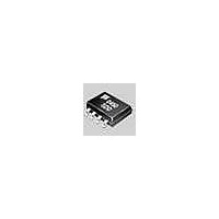
... CDNBS08-T03~T36C – TVS Diode Array Series Product Dimensions This is a molded JEDEC narrow body SO-8 package with lead free 100 % Sn plating on the lead frame. It weighs approximately 15 mg and has a flammability rating of UL 94V- Dimensions 4.80 - 5.00 A (0.189 - 0.196) 3.80 - 4.00 B (0.150 - 0.157) 5 ...

Page 3

... CDNBS08-T03~T36C – TVS Diode Array Series Performance Graphs Peak Pulse Power vs Pulse Time 10,000 500 W, 8/20 µs Waveform 1,000 100 10 0. 100 t – Pulse Duration (µs) d Block Diagram Unidirectional Bidirectional Device Pinout Pin Function GND 6 GND 7 GND 8 GND Specifications are subject to change without notice. ...

Page 4

... CDNBS08-T03~T36C – TVS Diode Array Series Packaging Specifications The product will be dispensed in Tape and Reel format (see diagram below Index Hole Trailer Device ....... ....... ....... ....... End ....... ....... ....... 10 pitches (min.) Item Symbol Carrier Width A Carrier Length B Carrier Depth C Sprocket Hole d Reel Outside Diameter D Reel Inner Diameter ...

Related keywords