EMLINK-BH EMBEST, EMLINK-BH Datasheet - Page 2
EMLINK-BH
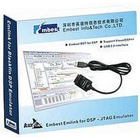
Manufacturer Part Number
EMLINK-BH
Description
Emlink USB To JTAG Emulator Module For Blackfin
Manufacturer
EMBEST
Datasheet
1.EMLINK-BH.pdf
(2 pages)
Specifications of EMLINK-BH
Silicon Family Name
Blackfin
Core Architecture
Blackfin
Ic Product Type
In-Circuit Emulator
Kit Contents
Emlink For Blackfin, JTAG20-14-8 Convert Module, IDC14 Cable, CD


prompt out window as following:
message such as: ‘…Process completed.’, then press Enter to finish, show as figure
5.2(a). The setup program will go on to copy and install Emlink driver for VDSP++. If the
last message gives out: ‘Completed’, installation has success and finish, show as figure
5.2(b).
EmlinkforVDSP++.exe installed success or not. If the installation was correct, the
reserved device ‘Legacy target’ was available (can be selected) as following.
Otherwise, the ‘Legacy target’ could not be selected (gray) if the Emlink driver install
failed.
appeared while connect Emlink to your target. Please check them like Figure 5.3.
JTAG port to connect to your target board’s JTAG port. Emlink can be power supplied via
PC’s USB port.
Embest Emlink ICE for Blackfin DSP
Hardware signals and ports
Emlink ICE for Blackfin
2. If one or more version of VisualDSP++ can be select, click ‘Install’ to continue, the
After a while, the Emlink USB driver should be installed to your windows, and display
3. Create a new Session under VisualDSP++ 4.5/4.0/5 to check if the
Figure 5.3 (a)Emlink target selection for VDSP++ Session
NOTES: If the Emlink USB driver installed failed, the error ‘0x80004005’ will be
Emlink has two sides, one is connected to PC through an USB port(Host), another is
Figure 5.2 (a) press Enter to exit USB installation (b) install completed and all 100%
can be plugged in directly.
user has to connect correct signal to Emlink JTAG port.
not pulled down with resistor this signal in board side (open or >10Kohm).
Emlink JTAG 20pins
NOTES for JTAG signal designed:
- It is recommended to design your target board as 20pins, then Emlink
- If designed to other pins (only connect the active signals’ pin), then
- There is 10Kohm resistor pulled up inside Emlink nTRST pin, please do
- All signal ‘GND’ should be connect to target board ground, 0V.
Figure 7.2 Emlink JTAG signal definition and connection
TMS
TDO
TDI
TCK
nTRST
EMU
GND
Vsupply
J1
DSP8
♦ Compatible with ADI
♦ Supports Blackfin BF53x processors,
♦ Debugging with Halt, Step, Run, Breakpoint
♦ Supports Windows98/NT/2000 /XP host
♦ Support
♦ Mini and smart size: 45x32x12mm, weight about 55g
♦ Power suply via USB port without power adapter
♦ JTAG port (20pins, FH2.54mm) for connecting target board
♦
♦ Support to program on-board Flash.
1
2
3
4
5
6
7
8
Features:
Downloading and debugging speed up to
Vref
nTRST
TDI
TMS
TCK
TDO
nSRST
EMU
USB 2.0
Completed
JP1_S
ARM10X2
1
3
5
7
9
11
13
15
17
19
protocol
10
12
14
16
18
20
2
4
6
8
VisualDSP++ 4.0/4.5/5.0
Hardware description
www.embedinfo.com/en
www.embedinfo.com/en
Vsupply
GND
GND
GND
GND
GND
GND
GND
GND
(b)Emlink device
GND
GND
200KBytes/s (1.5Mbps)
BF531/2/3/4/6/7
JTAG20-14-8 Module
JP3_D
DSP7X2
1
3
5
7
9
11
13
IDDE
10
12
14
2
4
6
8
etc.
5/8
7/8
EMU
GND
TMS
TCK
nTRST
TDI
TDO
☼
then the driver could be installed on the Windows system, the ‘Legacy target’ should be available to select.
☼
Flash.
☼ NOTES: ADI VisualDSP++ 4.0/4.5/5.0 are the commercial products provide by ADI,
customer should be authorized by ADI before using Emlink to debug your system.
interface. This document assumes a working knowledge of the JTAG specification.
appeared while connect Emlink to your target. Please check and resolve by:
them, please re-install EmlinkforVDSP++.exe again, and restart your windows once
after finished the installation, until there is no ‘?’ or ‘!’ on them. And the correct status of
these device show as figure 8.1(b).
TRST
TCK
TDI
TDO
TMS
nSRST
NC
GND
RES
Signal
Power supply
Emlink Connect Target
Refer to the IEEE 1149.1 JTAG specification for detailed information on the JTAG
Emlink can be power supplied via PC USB, without any power adapter.
Figure 8.1 (a)Emlink target selection for VDSP++ Session
NOTES: If the Emlink USB driver installed failed, the error ‘0x80004005’ will be
* check if there is ‘USB Serial Coverter A/B’ device under the list. if there is ? or ! on
Emlink driver for VisualDSP++ setup process is easy to understand: click EmlinkforVDSP++.exe to run,
Emlink ICE for Blackfin can use to debug BF531/2/3/4/6/7 target: debug source code in RAM or trace in
Input
Asynchronous
Input
Input
Output
Input
Input
X
X
X
Emlink for VDSP++
Type
Test Reset (JTAG): Resets the test state machine. The TRST signal must be
asserted after power up to ensure proper JTAG operation. The TRST signal has a
10 Kohm internal pull-up resistor. Please do not pulled down with resistor on
this pin in board side, but let it open or pulled download >10Kohm.
Test Clock (JTAG): Provides an asynchronous clock for JTAG boundary scan.
Test Data Input (JTAG): A serial data input of the boundary scan path. This
signal has a 10 kW internal pull-up resistor.
Test Data Output (JTAG): A serial data output of the boundary scan path.
Test Mode Select (JTAG): Controls the test state machine. This signal has a
10 kW internal pull-up resistor.
The target system reset signal. ICE can reset target via this signal.
No connect on Emlink side.
Ground.
Reserved.
Figure 6.1 Emlink for VDSP++ Connection Type
Figure 6.2 Session for BF53X + Emlink
Screen Shots and FAQs
Description
www.embedinfo.com/en
www.embedinfo.com/en
(b)Emlink device
6/8
8/8
Related parts for EMLINK-BH
Image
Part Number
Description
Manufacturer
Datasheet
Request
R

Part Number:
Description:
Emlink USB To JTAG Emulator Module For ARM
Manufacturer:
EMBEST
Datasheet:

Part Number:
Description:
ATMEL AT91SAM3U Starter Kit
Manufacturer:
EMBEST
Datasheet:

Part Number:
Description:
ATMEL AT91SAM3U ARM-CM3 Board
Manufacturer:
EMBEST
Datasheet:

Part Number:
Description:
NXP LPC1766 Evaluation Board
Manufacturer:
EMBEST
Datasheet:
Part Number:
Description:
NXP LPC1768 Evaluation Board
Manufacturer:
EMBEST
Datasheet:

Part Number:
Description:
STM32F103ZE ARM-CM3 Board
Manufacturer:
EMBEST
Datasheet:

Part Number:
Description:
LPC1766-SK ARM Starter Kit
Manufacturer:
EMBEST
Datasheet:
Part Number:
Description:
NXP LPC1768 Starter Kit
Manufacturer:
EMBEST
Datasheet:

Part Number:
Description:
Samsung S3C2440A Processor Card
Manufacturer:
EMBEST
Datasheet:

Part Number:
Description:
STM32F103ZE ARM-CM3 Starter Kit
Manufacturer:
EMBEST
Datasheet:

Part Number:
Description:
0.7 Inch 5*7 Dot Matrix Display
Manufacturer:
Everlight Electronic Co., Ltd.