IRPP3637-18A International Rectifier, IRPP3637-18A Datasheet
IRPP3637-18A
Specifications of IRPP3637-18A


Related parts for IRPP3637-18A


IRPP3637-18A Summary of contents
Page 1
... PCB layouts .........................................................................................7-8 Electrical Efficiency & Power Loss .......................................................9 Thermal Performance & Bode Plot.......................................................10 Input & Output Ripple Waveforms........................................................11 Load Step Waveforms..........................................................................12 Power Up & Power Down Waveforms..................................................13 Short Circuit Waveforms ......................................................................14 IRPP3637-xxA Reference Design Selector Table ................................14 www.irf.com Chipset Reference Design Table of Contents RD-0604 Page 1 ...
Page 2
... External is Vc bias. (Optional) (J5) +12V External Vc bias RTN (J6) Figure 1: IRPP3637-06A Electrical Connection Diagram Input/Output Connections J1: Input power connection terminal J2: Input power return preferred connection terminal J3: Output power return preferred connection terminal J4: Output terminal J5: External bias power connection terminal ...
Page 3
Start-Up Procedure The 5V input power is connected between terminals J1 and J2 and the 1.25V, 6A output power is obtained through terminals J3 and J4. The V and V pins are the low side CC C driver and high ...
Page 4
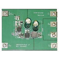
... Layout Considerations The IRPP3637-06A reference design PCB layout offers compact design with minimum parasitics at 600kHz switching frequency. The board is designed with 4 layers using 1 oz copper weight per layer. Figures 3a through 3d represent the layout of each layer. To minimize the parasitics, the following observed: 1 ...
Page 5
... Figure 2: Schematic Diagram for IRPP3637-06A Reference Design www.irf.com RD-0604 5 ...
Page 6
... Resistor,thick film,11kΩ Resistor,thick film,6.19kΩ, 1% Dual FET,20V,Q1/Q2=18.3mΩ,11nC 1 U1 PWM Controller 6 C2, C8, R4, R7, R9,R12 Not installed Table 1 – Complete Bill of Materials for IRPP3637-06A Reference Design www.irf.com SIZE MFR 0603 TDK 0603 KOA 0603 TDK 0603 TDK 1206 TDK 8mm X 16mm ...
Page 7
... Figure 3a: IRPP3637-06A Reference Design top layer placement and layout. Figure 3b: IRPP3637-06A Reference Design mid-layer1 ground plane www.irf.com RD-0604 7 ...
Page 8
... Figure 3c: IRPP3637-06A Reference Design mid-layer2 layout. Figure 3d: IRPP3637-06A Reference Design bottom layer layout. www.irf.com RD-0604 8 ...
Page 9
... Figure 4a: IRPP3637-06A Reference Design Electrical Efficiency IRPP3637AS-6A System Power Loss 5Vin, 1.25Vout, 600KHz, 25 2.00 1.75 1.50 1.25 1.00 0.75 0.50 0.25 0. Figure 4b: IRPP3637-06A Reference Design Power Loss Curve www.irf.com IRPP3637AS-6A Efficiency 0 C, 0LFM Load Current (Amps 0LFM Load Current (Amps) RD-0604 ...
Page 10
... Figure 5: IRPP3637-06A Reference Design Thermograph at 6A load Gain Ph =67 margin F = 57kHz o Figure 6: IRPP3637-06A Reference Design Bode Plot of the Control Loop at 6A load. www.irf.com IRF8910 Dual SO8 package -IR3637AS Vin=5V, Vo=1.25V, T =45 C Io= LFM Phase 0 RD-0604 ...
Page 11
Figure 8: Output ripple, I www.irf.com Figure 7: Input ripple, I =6A O =6A O RD-0604 11 ...
Page 12
Figure 9: Output Voltage undershoot due load step, di/dt=2.5A/us Figure 10: Output Voltage overshoot due load step, di/dt=2.5A/us www.irf.com RD-0604 12 ...
Page 13
Figure 11: Power up. Ch1=V Figure 12: Power down. Ch1=V www.irf.com , Ch2=V , Ch3=Soft Start IN OUT , Ch2=V , Ch3=Soft Start IN OUT RD-0604 13 ...
Page 14
... Voltage Voltage IRPP3637-06A 5V 1.25V IRPP3637-12A 12V 1.8V IRPP3637-18A 12V 3.3V Custom IRPP3637-06A 3.0V to Custom 0.8V to 5.0V 13.2V IRPP3637-12A Custom IRPP3637-18A Table 3 – Complete IRPP3637-xxA Reference Design Selector Table www.irf.com OUT Efficiency V V INripple OUTripple 0 ( %), 25 C, (mVp-p) (mVp-p) 0 LFM 80% 280mV 26mV (all values are typical) ...