HFBR-0555 Avago Technologies US Inc., HFBR-0555 Datasheet - Page 7
HFBR-0555
Manufacturer Part Number
HFBR-0555
Description
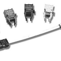
Fiber Optics, Evaluation Kit
Manufacturer
Avago Technologies US Inc.
Datasheet
1.HFBR-0555.pdf
(14 pages)
Specifications of HFBR-0555
Silicon Core Number
HFBR-5905/5905A
Features
Test Fixture (Footprint Compatible W/ All Multi-Mode 155 Megabit ATM Small Form Factor Transceivers)
Tool / Board Applications
Fiber Optic Transceivers
Main Purpose
Interface, Fiber Optics
Embedded
No
Utilized Ic / Part
HFBR-5900 Family
Primary Attributes
ATM Multimode Transceivers, 155Mbit
Secondary Attributes
SONET OC-3/SDH STM-1
Description/function
Fiber Optic Kit
Lead Free Status / RoHS Status
Lead free / RoHS Compliant
For Use With/related Products
HFCT-5903E
Lead Free Status / RoHS Status
Lead free / RoHS Compliant, Contains lead / RoHS non-compliant


Board Layout - Decoupling Circuit, Ground Planes and
Termination Circuits
It is important to take care in the layout of your circuit
board to achieve optimum performance from these
transceivers. Figure 7 provides a good example of a
schematic for a power supply decoupling circuit that
works well with these parts. It is further recommended
that a contiguous ground plane be provided in the
circuit board directly under the transceiver to provide
a low inductance ground for signal return current. This
recommendation is in keeping with good high
frequency board layout practices. Figures 7 and 8 show
two recommended termination schemes.
Figure 7. Recommended Decoupling and Termination Circuits
7
Note: C1 = C2 = C3 = 10 nF or 100 nF
T
R
X
X
TRANSCEIVER INPUTS
10
1
TERMINATE AT
2
9
3
8
130 Ω
4
7
100 Ω
5
6
130 Ω
C2
C1
1 µH
1 µH
Z = 50 Ω
Z = 50 Ω
V
C3
CC
Z = 50 Ω
Z = 50 Ω
Z = 50 Ω
(+3.3 V)
10 µF
Board Layout - Hole Pattern
The Avago Technologies transceiver complies with the
circuit board “Common Transceiver Footprint” hole
pattern defined in the original multisource announce-
ment which defined the 2 x 5 package style. This
drawing is reproduced in Figure 9 with the addition of
ANSI Y14.5M compliant dimensioning to be used as a
guide in the mechanical layout of your circuit board.
Board Layout - Art Work
The Applications Engineering group has developed a
Gerber file artwork for a multilayer printed circuit board
layout incorporating the recommendations above.
Contact your local Avago Technologies sales
representative for details.
130 Ω
130 Ω
V
DEVICE INPUTS
TERMINATE AT
82 Ω
CC
130 Ω
100 Ω
(+3.3 V)
TD-
TD+
RD+
RD-
SD
V
PHY DEVICE
CC
(+3.3 V)
LVPECL
LVPECL
V
CC
(+3.3 V)
Related parts for HFBR-0555
Image
Part Number
Description
Manufacturer
Datasheet
Request
R

Part Number:
Description:
Fiber Optic Transmitters, Receivers, Transceivers 1300nm 155MBd 16-pin DIP ST Rx
Manufacturer:
Avago Technologies US Inc.

Part Number:
Description:
FIBER OPTIC TX 125 MBD 650N
Manufacturer:
Avago Technologies US Inc.
Datasheet:

Part Number:
Description:
Fiber Optic Evaluation Kit
Manufacturer:
Avago Technologies US Inc.
Datasheet:

Part Number:
Description:
RECEIVER FIBER OPTIC ST 266MBD
Manufacturer:
Avago Technologies US Inc.
Datasheet:

Part Number:
Description:
RCVR OPT HI SPEED VERS LINK HORZ
Manufacturer:
Avago Technologies US Inc.
Datasheet:

Part Number:
Description:
RCVR OPT HI SPEED VERS LINK VERT
Manufacturer:
Avago Technologies US Inc.
Datasheet:

Part Number:
Description:
TXRX OPTICAL 850NM VCSEL MT-RJ
Manufacturer:
Avago Technologies US Inc.
Datasheet:

Part Number:
Description:
TXRX MM SFP LC CONN BAIL DELATCH
Manufacturer:
Avago Technologies US Inc.
Datasheet:

Part Number:
Description:
TXRX MMF SFP GBE/FC BAIL DELATCH
Manufacturer:
Avago Technologies US Inc.
Datasheet:

Part Number:
Description:
XMITTER FIBER OPTIC 266MBD ST
Manufacturer:
Avago Technologies US Inc.
Datasheet:

Part Number:
Description:
OPTOCOUPLER GATE DRV 2A 16-SOIC
Manufacturer:
Avago Technologies US Inc.
Datasheet:
Part Number:
Description:
OPTOCOUPLER 2CH 2.5A 16-SOIC
Manufacturer:
Avago Technologies US Inc.
Datasheet:

Part Number:
Description:
OPTOCOUPLER GATE DRV 0.4A 16SOIC
Manufacturer:
Avago Technologies US Inc.
Datasheet:

Part Number:
Description:
OPTOCOUPLER 2.0A 250KHZ 8-DIP
Manufacturer:
Avago Technologies US Inc.
Datasheet:

Part Number:
Description:
OPTOCOUPLER 2.0A 250KHZ GW 8-SMD
Manufacturer:
Avago Technologies US Inc.
Datasheet: