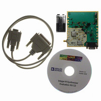
EVAL-ADF4106EBZ1 Analog Devices Inc, EVAL-ADF4106EBZ1 Datasheet
EVAL-ADF4106EBZ1
Specifications of EVAL-ADF4106EBZ1


Related parts for EVAL-ADF4106EBZ1


EVAL-ADF4106EBZ1 Summary of contents
Page 1
FEATURES 6.0 GHz bandwidth 2 3.3 V power supply Separate charge pump supply (V ) allows extended P tuning voltage systems Programmable dual-modulus prescaler 8/9, 16/17, 32/33, 64/65 Programmable charge pump currents Programmable antibacklash pulse ...
Page 2
ADF4106 TABLE OF CONTENTS Specifications ..................................................................................... 3 Timing Characterisitics ............................................................... 4 Absolute Maximum Ratings ............................................................ 5 ESD Caution .................................................................................. 5 Pin Configurations and Function Descriptions ........................... 6 Typical Performance Characteristics ............................................. 7 General Description ......................................................................... 9 Reference Input Section ............................................................... ...
Page 3
SPECIFICATIONS ± 10%, AV ≤ V ≤ 5.5 V, AGND = DGND = CPGND = unless otherwise noted. Table 1. Parameter RF CHARACTERISTICS RF Input Frequency (RF ...
Page 4
... − 10 log F PFD SYNTH TOT 12 The phase noise is measured with the EVAL-ADF4106EB1 evaluation board and the Agilent E4440A Spectrum Analyzer. The spectrum analyzer provides the REFIN for the synthesizer ( MHz @ 0 dBm). REFOUT MHz 200 kHz; Offset Frequency = 1 kHz; f ...
Page 5
ABSOLUTE MAXIMUM RATINGS T = 25°C, unless otherwise noted. A Table 3. Parameter GND GND Digital I/O Voltage to GND Analog I/O Voltage ...
Page 6
ADF4106 PIN CONFIGURATIONS AND FUNCTION DESCRIPTIONS SET CPGND ADF4106 TOP VIEW 4 13 AGND (Not to Scale REF ...
Page 7
TYPICAL PERFORMANCE CHARACTERISTICS FREQ UNIT GHz KEYWORD R PARAM TYPE S IMPEDANCE 50Ω DATA FORMAT MA FREQ MAGS11 ANGS11 FREQ MAGS11 ANGS11 0.500 0.89148 –17.2820 3.300 0.42777 0.600 0.88133 – 20.6919 3.400 0.42859 0.700 0.87152 – 24.5386 3.500 0.43365 0.800 ...
Page 8
ADF4106 –40 –50 –60 –70 –80 –90 –100 –110 –120 –130 –140 100Hz FREQUENCY OFFSET FROM 5800MHz CARRIER Figure 11. Integrated Phase Noise (5.8 GHz,1 MHz, and 100 kHz 3V, V REF LEVEL = –10dBm DD I ...
Page 9
GENERAL DESCRIPTION REFERENCE INPUT SECTION The reference input stage is shown in Figure 17. SW1 and SW2 are normally closed switches. SW3 is a normally open switch. When power-down is initiated, SW3 is closed and SW1 and SW2 are opened. ...
Page 10
ADF4106 PHASE FREQUENCY DETECTOR (PFD) AND CHARGE PUMP The PFD takes inputs from the R counter and N counter ( and produces an output proportional to the phase and frequency difference between them. Figure 20 is ...
Page 11
Table 6. Latch Summary ANTI- TEST BACKLASH RESERVED MODE BITS WIDTH DB23 DB22 DB21 DB20 DB19 DB18 DB17 DB16 DB15 DB14 DB13 DB12 DB11 DB10 LDP T2 T1 ABP2 RESERVED DB23 DB22 DB21 DB20 DB19 DB18 DB17 ...
Page 12
ADF4106 Table 7. Reference Counter Latch Map TEST BACKLASH RESERVED MODE BITS DB23 DB22 DB21 DB20 DB19 DB18 DB17 DB16 DB15 DB14 DB13 DB12 DB11 DB10 0 0 LDP T2 T1 ABP2 DON’T CARE ABP2 0 0 ...
Page 13
Table 8. N (A, B) Counter Latch Map RESERVED DB21 DB19 DB23 DB22 DB20 DB18 DB17 B13 B12 B11 B10 X = DON’T CARE B13 B12 B11 ...
Page 14
ADF4106 Table 9. Function Latch Map CURRENT CURRENT PRESCALER SETTING SETTING VALUE 2 DB23 DB22 DB21 DB20 DB19 DB18 DB17 DB16 DB15 DB14 DB13 DB12 DB11 DB10 P2 P1 PD2 CPI6 CPI5 CPI4 CPI3 CPI2 TC4 ...
Page 15
Table 10. Initialization Latch Map CURRENT CURRENT PRESCALER SETTING SETTING VALUE 2 DB23 DB22 DB21 DB20 DB19 DB18 DB17 DB16 DB15 DB14 DB13 DB12 DB11 DB10 P2 P1 PD2 CPI6 CPI5 CPI4 CPI3 CPI2 TC4 ...
Page 16
ADF4106 THE FUNCTION LATCH With C2 and C1 set to 1 and 0, respectively, the on-chip function latch is programmed. Table 9 shows the input data format for programming the function latch. Counter Reset DB2 (F1) is the counter reset ...
Page 17
Charge Pump Currents CPI3, CPI2, and CPI1 program Current Setting 1 for the charge pump. CPI6, CPI5, and CPI4 program Current Setting 2 for the charge pump. The truth table is given in Table 9. Prescaler Value P2 and P1 ...
Page 18
ADF4106 APPLICATIONS LOCAL OSCILLATOR FOR LMDS BASE STATION TRANSMITTER Figure 22 shows the ADF4106 being used with a VCO to produce the LO for an LMDS base station. The reference input signal is applied to the circuit at FREF and, ...
Page 19
INTERFACING The ADF4106 has a simple SPI-compatible serial interface for writing to the device. CLK, DATA, and LE control the data transfer. When LE goes high, the 24 bits clocked into the input register on each rising edge of CLK ...
Page 20
ADF4106 OUTLINE DIMENSIONS 0.15 0.05 PIN 1 INDICATOR 12° MAX 1.00 0.85 0.80 SEATING PLANE 5.10 5.00 4. 4.50 6.40 4.40 BSC 4. PIN 1 1.20 MAX 0.20 0.09 8° 0.30 0° 0.65 0.19 SEATING BSC ...
Page 21
... ADF4106BCPZ –40° 85°C ADF4106BCPZ-RL –40° 85°C ADF4106BCPZ-R7 –40° 85°C EVAL-ADF4106EBZ1 EVAL-ADF411XEBZ1 RoHS Compliant. Package Description 16-Lead Thin Shrink Small Outline Package (TSSOP) 16-Lead Thin Shrink Small Outline Package (TSSOP) 16-Lead Thin Shrink Small Outline Package (TSSOP) ...
Page 22
ADF4106 NOTES Rev Page ...
Page 23
NOTES Rev Page ADF4106 ...
Page 24
ADF4106 NOTES ©2001–2010 Analog Devices, Inc. All rights reserved. Trademarks and registered trademarks are the property of their respective owners. D02720-0-2/10(C) Rev Page ...