LM3409EVAL/NOPB National Semiconductor, LM3409EVAL/NOPB Datasheet - Page 6
LM3409EVAL/NOPB
Manufacturer Part Number
LM3409EVAL/NOPB
Description
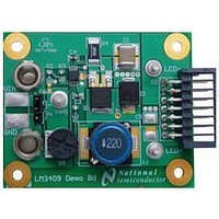
LED Driver Demo Board
Manufacturer
National Semiconductor
Datasheet
1.LM3409HVEVAL.pdf
(10 pages)
Specifications of LM3409EVAL/NOPB
Core Chip
LM3409
Topology
Buck (Step Down)
No. Of Outputs
1
Dimming Control Type
PWM
Tool / Board Applications
Lighting-LED, High Bright LED, LED Driver, Flourescent, Backlighting
Development Tool Type
Hardware - Eval/Demo Board
Mcu Supported Families
LM3409 Family


www.national.com
10. PWM DIMMING METHOD
The LM3409HV evaluation board allows for PWM dimming to
be evaluated as follows:
Method #1: If no PWM dimming is desired, a jumper should
be placed in position 1 (shorts pins 1 and 2) on header J1.
This shorts VIN and EN which ensures the controller is always
enabled if an input voltage greater than 1.74V is applied.
Method #2: External parallel FET shunt dimming can be eval-
uated by placing the jumper in position 2 (shorts pins 2 and
3) on header J1. This connects the capacitive coupling circuit
to the EN pin as suggested in the datasheet. The resistor (R4)
can be solved for assuming a standard capacitor value C9 =
2.2nF and a desired time constant (t
lows:
The external shunt FET dimming circuit shown below is de-
signed using an N-channel MosFET (Q3), a CMOS FET (Q2),
two gate current limiting resistors (R1 and R2), a pull-up re-
sistor (R3), and a bypass capacitor (C5). With an external 5V
power supply attached to the 5V terminal and an external
PWM signal attached to the PWM2 terminal, the shunt dim-
ming circuit is complete. Q3 is the shunt dimFET which con-
ducts the LED current when turned on and blocks the LED
voltage when turned off. Q3 needs to be fast and rated for
V
chosen. Q2 is necessary to invert the PWM signal so it prop-
O
and I
LED
. For design flexibility, a fast 100V, 7.5A NFET is
External shunt FET dimming circuit with EN pin coupling
C
= 220ns < t
OFF
30093502
) as fol-
6
erly translates the duty cycle to the shunt dimming FET. Q2
also needs to be fast and rated for 5V and fairly small current,
therefore a 30V, 2A fast CMOS FET was chosen. R1 and R2
are 1Ω resistors to slow down the rising edge of the FETs
slightly to prevent the gate from ringing. R3 is a 10kΩ pull-up
resistor to ensure the CMOS gate is pulled all the way to 5V
if a sub-5V PWM signal is applied to PWM2. The bypass ca-
pacitor (C5) for the 5V power supply is chosen to be 0.1µF.
See the Shunt FET Circuit Modification section for an im-
provement that can be made to this circuit.
Method #3: Internal PWM dimming using the EN pin can be
evaluated by removing the jumper from header J1. An exter-
nal PWM signal can then be applied to the EN terminal to
provide PWM dimming.
The Typical Waveforms section shows typical LED current
waveforms during both types of PWM dimming.
The chosen components from step 10 are:
11. BYPASS CAPACITOR
The internal regulator requires at least 1µF of ceramic capac-
itance with a voltage rating of 16V.
The chosen component from step 11 is:
30093533
Related parts for LM3409EVAL/NOPB
Image
Part Number
Description
Manufacturer
Datasheet
Request
R

Part Number:
Description:
LM3409 LM3409HV PFET Buck Controller for High Power LED Drives; Package: MINI SOIC EXP PAD; No of Pins: 10; Qty per Container: 1000/Reel
Manufacturer:
National Semiconductor
Datasheet:
Part Number:
Description:
LM3409 LM3409HV PFET Buck Controller for High Power LED Drives; Package: MINI SOIC EXP PAD; No of Pins: 10; Qty per Container: 3500/Reel
Manufacturer:
National Semiconductor
Datasheet:
Part Number:
Description:
National Semiconductor [8-Bit D/A Converter]
Manufacturer:
National Semiconductor
Datasheet:
Part Number:
Description:
National Semiconductor [Media Coprocessor]
Manufacturer:
National Semiconductor
Datasheet:
Part Number:
Description:
Digitally Controlled Tone and Volume Circuit with Stereo Audio Power Amplifier, Microphone Preamp Stage and National 3D Sound
Manufacturer:
National Semiconductor
Datasheet:
Part Number:
Description:
Digitally Controlled Tone and Volume Circuit with Stereo Audio Power Amplifier, Microphone Preamp Stage and National 3D Sound
Manufacturer:
National Semiconductor
Datasheet:
Part Number:
Description:
AC97 Rev 2 Codec with Sample Rate Conversion and National 3D Sound
Manufacturer:
National Semiconductor
Part Number:
Description:
Manufacturer:
National Semiconductor
Datasheet:
Part Number:
Description:
Manufacturer:
National Semiconductor
Datasheet:
Part Number:
Description:
General Purpose, Low Voltage, Low Power, Rail-to-Rail Output Operational Amplifiers
Manufacturer:
National Semiconductor
Datasheet:
Part Number:
Description:
8-bit 20 MSPS flash A/D converter.
Manufacturer:
National Semiconductor
Datasheet:
Part Number:
Description:
Low Noise Quad Operational Amplifier
Manufacturer:
National Semiconductor
Datasheet:
Part Number:
Description:
Quad Differential Line Receivers
Manufacturer:
National Semiconductor
Datasheet:
Part Number:
Description:
Quad High Speed Trapezoidal? Bus Transceiver
Manufacturer:
National Semiconductor
Datasheet: