CFPT-9000 Series
ISSUE 9 ; 3 MARCH 2005
Recommended for New Designs
Delivery Options
I
Description
I
RoHS compliance
I
Standard Frequencies
I
Output Waveform
I
I
I
I
Supply Voltage
I
Current Consumption
I
I
I
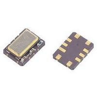
Package Outline
I
Parts with the suffix ‘LF’ on the ordering code and part
Please contact our sales office for current leadtimes
A series of surface mountable 7.0
compensated voltage controlled crystal oscillators
(TCVCXOs) for medium to high volume applications
where small size and high performance are pre-
requisites. This oscillator uses C-MAC’s latest custom
ASIC "Pluto", a single chip oscillator and analogue
compensation circuit, capable of sub 1 ppm
performance over an extended temperature range. Its
ability to function down to a supply voltage of 2.4V and
low power consumption make it particularly suitable for
mobile applications
number are fully compliant with the European Union
directive 2002/95/EC on the restriction of the use of
certain hazardous substances in electrical and
electronic equipment. Note: The RoHS compliant parts
are suitable for assembly using both Lead-free solders
(see Lead-free Reflow soldering profile) and Tin / Lead
solders (see Tin / Lead Reflow soldering profile).
3.2, 5.0, 6.4, 8.192, 9.6, 12.688375, 10.0, 12.8, 13.0, 14.4,
14.85, 16.384, 16.367, 16.8, 19.2, 19.44, 19.8, 20.0,
24.5535, 32.768, 38.88, 40.0MHz
Square HCMOS 15pF load
Square ACMOS 50pF max. load
(available on request, contact sales office)
Sinewave 10kΩ // 10pF , AC-coupled
Clipped sinewave 10kΩ // 10pF , AC-coupled
Operating range 2.4 to 6.0V, see table
HCMOS Typically
1+Frequency(MHz)*Supply(V)*{Load(pF)+15}*10 -3 mA
e. g. 20MHz, 5V, 15pF
Sinewave, < 8mA
Clipped Sinewave Typically ≈
1+Frequency(MHz)*1.2*{Load(pF)+30}*10 -3 mA
7.0 x 5.0 x 2.0mm SMD Ceramic Carrier
≈
≈
4mA
×
5.0mm temperature
248
Ageing
I
I
I
I
I
Frequency Stability
I
I
I
Frequency Adjustment
I
I
I
I
I
I
Reference Voltage, Vref
I
For manual frequency adjustment connect an external
50kΩ potentiometer between pad 1 (Reference Voltage)
and pad 4 (GND) with wiper connected to pad 10 (Voltage
Control). Please specify reference voltage as part of the
ordering code
±1ppm maximum in first year, frequency < 20MHz
±2ppm maximum in first year, frequency > 20MHz
±3ppm maximum for 10 years, frequency < 20MHz
±5ppm maximum for 10 years, frequency > 20MHz
±1ppm maximum after reflow
Temperature: see table
Typical Supply Voltage Variation ±10% < ±0.2 ppm*
Typical Load Coefficient 15pF ±5pF < ±0.2 ppm*
Three options with external Voltage Control applied to
pad 10:
A - Ageing adjustment: > ±5ppm, frequency < 20MHz
B - No frequency adjustment initial calibration @ 25°C
C - High Pulling ±10ppm to ±50ppm can be available
Linearity
Slope
Input resistance
Modulation bandwidth
Standard voltage control ranges:
Optional reference voltage output on pad 1, suitable for
potentiometer supply or DAC reference.
1. No output (standard option)
2. 2.2V, for Min. Vs>2.4V
3. 2.7V, for Min. Vs>3.0V
4. 4.2V, for Min. Vs>4.5V
Maximum load current (mA) = Vref /10
Without reference voltage
Without reference voltage
With reference voltage
*Dependent on frequency and output type
< ±1.0 ppm
depending on frequency and stability options.
Please consult our sales office
(Standard Option)
> ±7ppm, frequency > 20MHz
- Vs=5.0V 2.5V±1V
- Vs=3.3V 1.65V±1V
- Vc=0V to Vref
< 1%
Positive
> 100kΩ
> 2kHz