660EVAL RF Solutions, 660EVAL Datasheet - Page 5
660EVAL
Manufacturer Part Number
660EVAL
Description
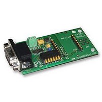
BOARD, EVALUATION
Manufacturer
RF Solutions
Datasheet
1.660EVAL.pdf
(11 pages)
Specifications of 660EVAL
Svhc
No SVHC (15-Dec-2010)
Lead Free Status / RoHS Status
Lead free / RoHS Compliant


DS650-6 June ‘06
3
The configuration of the RF650 module may be changed by setting the Configuration pin low, then sending a
set of configuration data bytes to the module on the Tx pin.
Alternatively the Configuration software can be used to setup the module through a graphical interface, please
refer to section 3.1 for details on this.
The RF Channel is calculated as:
433 MHz working frequency: Config value (decimal) = (desired RF frequency - 422.4MHz) * 10
868 MHz working frequency: Config value (decimal) = [(desired RF frequency / 2) - 422.4MHz] * 10
Please Note, the calculated value must be converted into hexadecimal format.
The Configuration pin must be held low for at least the first byte to change the RF650 module into
configuration mode. If the Configuration pin is still low at the end of the configuration then the module
will send the current configuration back to the host. To retrieve the current configuration without
changing any options the host can send a single byte to the module and wait for the response.
It is not necessary to send all configuration bytes to the module, but all data sent must be valid. For example
to change the destination address the host may just send four bytes. Configuration data excluded from the end
of the data stream will be unchanged. The RF650 module will accept a short configuration after a 10ms
timeout after the last byte sent to the module, or when the RTS pin goes high. This allows for the host to easily
change the destination address of the RF data packet, thus enabling one RF650 to send individual data to
several different recipient modules.
A destination address of 00000000 will reset the RF650 to the default settings shown above.
RF data packets received by the RF650 with the embedded destination address which matches the RF650
address will be accepted, processed and passed to the host, all of the RF data packets will be ignored.
When configuring the destination or RF650 address an incorrect number of bytes for an address will leave the
current address unchanged.
An invalid Transmitter Power or Packet Size setting will leave the current setting unchanged.
Byte
10
11
0
1
2
3
4
5
6
7
8
9
Configuration
Destination Address
Rx data packet size
Tx data packet size
RF650 Address
RF Channel
Tx Power
©2006 RF Solutions Ltd, www.rfsolutions.co.uk
Name
Tel 01273 898000 Fax 01273 480661
S
MART
MSB
LSB
MSB
LSB
100 kHz step offset from 422.4MHz
0 = -10dBm
1 = -2dBm
2 = +6dBm
3 = +10dBm
1 – 31 bytes
1 – 31 bytes
R
ADIO
Description
T
RANSCEIVER
Page 5
7E hex
7E hex
7E hex
7E hex
7E hex
7E hex
7E hex
7E hex
107 (433.1MHz)
0 (-10dBm)
30 bytes
30 bytes
Default Supplied Value
RF650
Related parts for 660EVAL
Image
Part Number
Description
Manufacturer
Datasheet
Request
R

Part Number:
Description:
RF Switch SPDT 0MHz to 2GHz 27dB 8-Pin SOIC T/R
Manufacturer:
M/A-Com Technology Solutions
Datasheet:
Part Number:
Description:
RF Switch SPST 500MHz to 2GHz 40dB 8-Pin SOIC T/R
Manufacturer:
M/A-Com Technology Solutions
Datasheet:

Part Number:
Description:
RF Switch SPDT 100MHz to 4GHz 14dB 6-Pin SOT-6
Manufacturer:
Skyworks Solutions Inc
Datasheet:
Part Number:
Description:
RF Switch SPST 500MHz to 2.5GHz 10dB 6-Pin SOT-6
Manufacturer:
Skyworks Solutions Inc

Part Number:
Description:
IC ENCODER TRANSMITTER RF 8DIP
Manufacturer:
RF Solutions
Datasheet:

Part Number:
Description:
IC DECODER RECEIVER RF 18DIP
Manufacturer:
RF Solutions
Datasheet:

Part Number:
Description:
IC ENCODER 3 DGTL I/O SOT23-6
Manufacturer:
RF Solutions
Datasheet:

Part Number:
Description:
IC ENCODER 3 DGTL I/O 8-PDIP
Manufacturer:
RF Solutions
Datasheet:

Part Number:
Description:
IC DECODER 3 DGTL I/O 8-PDIP
Manufacturer:
RF Solutions
Datasheet:

Part Number:
Description:
IC DECODER 3 DGTL I/O 8-SOIC
Manufacturer:
RF Solutions
Datasheet:

Part Number:
Description:
118 SERIES AM REMOTE CONTROL SYSTEMS.
Manufacturer:
RF Solutions Ltd.