AMMP-6222-TR2G Avago Technologies US Inc., AMMP-6222-TR2G Datasheet - Page 2
AMMP-6222-TR2G
Manufacturer Part Number
AMMP-6222-TR2G
Description
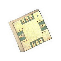
7-21GHz Hi Lin LNA In SMT Pkg
Manufacturer
Avago Technologies US Inc.
Datasheet
1.AMMP-6222-TR2G.pdf
(12 pages)
Specifications of AMMP-6222-TR2G
Current - Supply
120mA
Frequency
7GHz ~ 21GHz
Gain
24dB
Noise Figure
2.3dB
P1db
15.5dBm
Package / Case
8-SMD
Rf Type
WiMax
Voltage - Supply
3 V ~ 5 V
Number Of Channels
1
Power Supply Requirement
Single
Single Supply Voltage (min)
3V
Single Supply Voltage (typ)
4V
Single Supply Voltage (max)
5V
Package Type
SMD
Dual Supply Voltage (min)
Not RequiredV
Dual Supply Voltage (typ)
Not RequiredV
Dual Supply Voltage (max)
Not RequiredV
Supply Current
160@4VmA
Pin Count
8
Mounting
Surface Mount
Lead Free Status / RoHS Status
Lead free / RoHS Compliant
Test Frequency
-
Lead Free Status / Rohs Status
Compliant
Available stocks
Company
Part Number
Manufacturer
Quantity
Price

Part Number:
AMMP-6222-TR2G
Manufacturer:
AVAGO/安华高
Quantity:
20 000


Absolute Maximum Ratings
1. Operation in excess of any of these conditions may result in permanent damage to this device. The absolute maximum ratings for Vdd, Idd and Pin
DC Specifications/ Physical Properties
2. Ambient operational temperature TA=25°C unless noted
3. Channel-to-backside Thermal Resistance (Tchannel = 34°C) as measured using infrared microscopy.
AMMP-6222 RF Specifications
TA= 25°C, Idd=120mA, Vdd = 4.0 V, Zo=50 :
4. Refer to characteristic plots for detailed individual frequency performance.
5. All tested parameters guaranteed with measurement accuracy ± 0.5dB for gain and ±0.3dB for NF in the high output power configuration.
2
Parameters/Condition
Drain to Ground Voltage
Drain Current
RF CW Input Power Max
Max channel temperature
Storage temperature
Maximum Assembly Temp
Parameter and Test Condition
Drain Supply Current under any RF power drive and temp. (Vd=4.0 V)
Drain Supply Voltage
Thermal Resistance
Parameters and Test Conditions
Drain Current
Small-Signal Gain
Noise Figure into 50
Output Power at 1dB Gain Compression
Output Power at 3dB Gain Compression
Output Third Order Intercept Point
Isolation
Input Return Loss
Output Return Loss
were determined at an ambient temperature of 25°C unless noted otherwise.
Thermal Resistance at backside temp. (Tb) = 25°C calculated from measured data.
(5)
(3)
: (5)
(1)
(4)
Symbol
Vdd
Idd
Pin
Tch
Tstg
Tmax
Symbol
Idd
Gain
NF
P-1dB
P-3dB
OIP3
Iso
RLin
RLout
(2)
Unit
V
mA
dBm
C
C
C
Units
mA
dB
dB
dBm
dBm
dBm
dB
dB
dB
Freq.
(GHz)
9, 12, 17
9, 12, 17
Maximum
5.5
170
10
+150
-65 +150
260 for 20s
Symbol
Idd
Vd
θjc
High Output Power Configuration
Minimum
19
Typical
120
24
2.3
15.5
17.5
29
-45
-10
-10
Unit
mA
V
°C/W
Maximum
3.5
Minimum
80
3
Low Output Power Configuration
Minimum Typical
Typical
120
4
31.4
95
23
2.3
14
16
27
-45
-10
-10
Maximum
160
5
Maximum
Related parts for AMMP-6222-TR2G
Image
Part Number
Description
Manufacturer
Datasheet
Request
R

Part Number:
Description:
IC MMIC AMP LNA 7GHZ-21GHZ 8SMD
Manufacturer:
Avago Technologies US Inc.
Datasheet:
Part Number:
Description:
IC MMIC AMP LNA 7GHZ-21GHZ 8SMD
Manufacturer:
Avago Technologies US Inc.
Datasheet:

Part Number:
Description:
IC AMP GP HI PWR 6-20GHZ 8-SMD
Manufacturer:
Avago Technologies US Inc.
Datasheet:

Part Number:
Description:
IC AMP GP HI PWR 6-20GHZ 8-SMD
Manufacturer:
Avago Technologies US Inc.
Datasheet:

Part Number:
Description:
IC MMIC AMP HGA 6-20GHZ 8SMD
Manufacturer:
Avago Technologies US Inc.
Datasheet:

Part Number:
Description:
IC MMIC AMP HGA 6-20GHZ 8SMD
Manufacturer:
Avago Technologies US Inc.
Datasheet:
Part Number:
Description:
IC MMIC LOW NOISE 6-20GHZ 8-SMD
Manufacturer:
Avago Technologies US Inc.
Datasheet:
Part Number:
Description:
IC AMP GP HI PWR 6-20GHZ 8-SMD
Manufacturer:
Avago Technologies US Inc.
Datasheet:

Part Number:
Description:
6-20 GHz High Gain Amp In SMT Pkg
Manufacturer:
Avago Technologies US Inc.
Datasheet:

Part Number:
Description:
Power Amp, MMIC, 6-18GHz Pkg
Manufacturer:
Avago Technologies US Inc.
Datasheet:

Part Number:
Description:
OPTOCOUPLER GATE DRV 2A 16-SOIC
Manufacturer:
Avago Technologies US Inc.
Datasheet:
Part Number:
Description:
OPTOCOUPLER 2CH 2.5A 16-SOIC
Manufacturer:
Avago Technologies US Inc.
Datasheet:

Part Number:
Description:
OPTOCOUPLER GATE DRV 0.4A 16SOIC
Manufacturer:
Avago Technologies US Inc.
Datasheet:

Part Number:
Description:
OPTOCOUPLER 2.0A 250KHZ 8-DIP
Manufacturer:
Avago Technologies US Inc.
Datasheet:

Part Number:
Description:
OPTOCOUPLER 2.0A 250KHZ GW 8-SMD
Manufacturer:
Avago Technologies US Inc.
Datasheet: