AMMP-5620-TR2G Avago Technologies US Inc., AMMP-5620-TR2G Datasheet - Page 11
AMMP-5620-TR2G
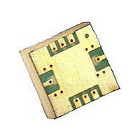
Manufacturer Part Number
AMMP-5620-TR2G
Description
6-20 GHz High Gain Amp In SMT Pkg
Manufacturer
Avago Technologies US Inc.
Datasheet
1.AMMP-5620-TR2G.pdf
(12 pages)
Specifications of AMMP-5620-TR2G
Current - Supply
95mA
Frequency
6GHz ~ 20GHz
Gain
17.5dB
Noise Figure
5.1dB
P1db
14.8dBm
Package / Case
8-SMD
Rf Type
General Purpose
Test Frequency
18GHz
Voltage - Supply
5V
Number Of Channels
1
Frequency (max)
20GHz
Power Supply Requirement
Single
Single Supply Voltage (typ)
5V
Package Type
SMT
Dual Supply Voltage (min)
Not RequiredV
Dual Supply Voltage (typ)
Not RequiredV
Dual Supply Voltage (max)
Not RequiredV
Supply Current
130mA
Pin Count
8
Mounting
Surface Mount
Lead Free Status / RoHS Status
Lead free / RoHS Compliant
Lead Free Status / RoHS Status
Lead free / RoHS Compliant
Available stocks
Company
Part Number
Manufacturer
Quantity
Price

Part Number:
AMMP-5620-TR2G
Manufacturer:
AVAGO/安华高
Quantity:
20 000


Stencil Design Guidelines
A properly designed solder screen or stencil is required
to ensure optimum amount of solder paste is deposited
onto the PCB pads. The recommended stencil layout is
shown in Figure 26. The stencil has a solder paste deposi-
tion opening approximately 70% to 90% of the PCB pad.
Reducing stencil opening can potentially generate more
voids underneath. On the other hand, stencil openings
larger than 100% will lead to excessive solder paste smear
or bridging across the I/O pads. Considering the fact that
solder paste thickness will directly affect the quality of
the solder joint, a good choice is to use a laser cut stencil
composed of 0.127 mm (5 mils) thick stainless steel which
is capable of producing the required fine stencil outline.
The combined PCB and stencil layout is shown in Figure
27.
Figure 25. Suggested PCB Land Pattern and Stencil Layout
Figure 26. Stencil Outline Drawing (mm)
Figure 27. Combined PCB and Stencil Layout
Related parts for AMMP-5620-TR2G
Image
Part Number
Description
Manufacturer
Datasheet
Request
R

Part Number:
Description:
IC MMIC AMP HGA 6-20GHZ 8SMD
Manufacturer:
Avago Technologies US Inc.
Datasheet:

Part Number:
Description:
IC MMIC AMP HGA 6-20GHZ 8SMD
Manufacturer:
Avago Technologies US Inc.
Datasheet:

Part Number:
Description:
IC AMP LN 5X5MM SMD
Manufacturer:
Avago Technologies US Inc.
Datasheet:

Part Number:
Description:
IC AMP GP HI PWR 6-20GHZ 8-SMD
Manufacturer:
Avago Technologies US Inc.
Datasheet:

Part Number:
Description:
IC MMIC REJECT MXR 5-30GHZ 8-SMD
Manufacturer:
Avago Technologies US Inc.
Datasheet:
Part Number:
Description:
IC MMIC REJECT MXR 5-30GHZ 8-SMD
Manufacturer:
Avago Technologies US Inc.
Datasheet:
Part Number:
Description:
IC MMIC REJECT MXR 5-30GHZ 8-SMD
Manufacturer:
Avago Technologies US Inc.
Datasheet:

Part Number:
Description:
IC MMIC LNA 18GHZ-31GHZ 8SMD
Manufacturer:
Avago Technologies US Inc.
Datasheet:

Part Number:
Description:
IC MMIC PWR AMP 30GHZ 8SMD
Manufacturer:
Avago Technologies US Inc.
Datasheet:

Part Number:
Description:
IC MMIC AMP LNA 7GHZ-21GHZ 8SMD
Manufacturer:
Avago Technologies US Inc.
Datasheet:

Part Number:
Description:
OPTOCOUPLER GATE DRV 2A 16-SOIC
Manufacturer:
Avago Technologies US Inc.
Datasheet:
Part Number:
Description:
OPTOCOUPLER 2CH 2.5A 16-SOIC
Manufacturer:
Avago Technologies US Inc.
Datasheet:

Part Number:
Description:
OPTOCOUPLER GATE DRV 0.4A 16SOIC
Manufacturer:
Avago Technologies US Inc.
Datasheet:

Part Number:
Description:
OPTOCOUPLER 2.0A 250KHZ 8-DIP
Manufacturer:
Avago Technologies US Inc.
Datasheet:

Part Number:
Description:
OPTOCOUPLER 2.0A 250KHZ GW 8-SMD
Manufacturer:
Avago Technologies US Inc.
Datasheet: