DD-25664YW-4A DENSITRON, DD-25664YW-4A Datasheet - Page 10
DD-25664YW-4A
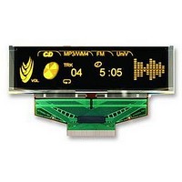
Manufacturer Part Number
DD-25664YW-4A
Description
DISPLAY, OLED, 64X256, YELLOW
Manufacturer
DENSITRON
Datasheet
1.DD-25664YW-4A.pdf
(27 pages)
Specifications of DD-25664YW-4A
Screen Size
79.248mm
Resolution
256 X 64
Viewing Area (h X W)
21.18mm X 78.78mm
Pixel Size (h X W)
0.28mm X 0.28mm
Voltage Rating
2.8V
External Depth
2.2mm
External Length / Height
27.8mm
Svhc
No SVHC (15-Dec-2010)
Rohs Compliant
Yes
Display Technology
Organic LED
Interface Type
Parallel, Serial
Lead Free Status / RoHS Status
Lead free / RoHS Compliant


Copyright ©2008 DENSITRON TECHNOLOGIES plc. All rights reserved. – Proprietary Data
18
19
20
21
22
23
24
25
26
27
28
29
30
Product No.
N.C. (GND)
VDDIO
VLSS
RES#
D/C#
IREF
VDD
VCC
N.C.
VSL
CS#
VCI
FR
DD-25664YW-4A
O
O
P
P
P
P
P
P
P
P
P
P
I
I
I
I
-
I
-
I
I
-
I
-
D
C
P
C
This pin is No Connection pins. Nothing should be connected to this
pin. It should be left open individually.
C
This pin is segment current reference pin. A resistor should be
connected between this pin and VSS. Set the current lower than
10
R
The N.C. pin between function pins are reserved for compatible and
flexible design.
P
This pin is a power supply pin of I/O buffer. It should be connected
to VDD or external source. All I/O signals should have VIH
reference to VDDIO. When I/O signal pins (BS0~BS1, D0~D7,
control signals…) pull high, they should be connected to VDDIO.
P
This is a voltage supply pin. It can be supplied externally (within the
range of 2.4~2.6V) or regulated internally from VCI. A capacitor
should be connected between this pin & VSS under all
circumstances.
P
This is a voltage supply pin. It must be connected to external source
& always be equal or higher than VDD & VDDIO.
V
This is segment voltage reference pin.
When external VSL is not used, this pin should be left open.
When external VSL is used, this pin should connect with resistor and
diode to ground.
G
This is the analog ground pin. It should be connected to VSS
externally
P
This is the most positive supply pin of the chip. They should be
connected to external source.
R
function pins. This pin must be connected to external ground.
D
C
P
C
C
R
P
P
P
V
G
P
R
The supporting pins can reduce the influences from stresses on the
This pin is Data/Command control pin. When the pin is pulled high,
the input at D7~D0 is treated as display data. When the pin is
pulled low, the input at D7~D0 will be transferred to the command
register. For detailed relationship to MCU interface signals, please
refer to the Timing Characteristics Diagrams
This pin is the chip select input. When the pin is enabled for MCU
communication only when CS# is pulled low..
This pin is reset signal input. When the pin is low, initialization of
the chip is executed.
h
o
o
a
u
e
e
o
o
o
o
o
o
o
o
o
o
e
e
h
a
u
a
a
r
r
µA
s
s
s
s
w
w
w
w
w
w
w
w
l
l
o
o
w
w
i
i
s
s
r
r
t
t
t
t
p
p
e
e
e
e
a
a
c
c
r
r
u
a
a
u
e
e
e
e
e
e
e
e
e
e
r
r
r
r
e
/
a
e
/
a
n
S
g
n
S
r
r
r
r
g
r
C
r
v
r
r
r
r
v
C
v
v
n
n
d
d
d
e
d
e
e
e
e
e
e
e
R
S
S
S
S
R
t
S
S
S
S
o
t
o
e
e
l
l
d
d
d
d
u
u
u
u
u
u
O
O
o
u
u
m
e
e
R
R
o
m
e
e
A
A
c
p
p
p
p
p
p
f
p
p
c
s
s
P
P
f
P
P
e
e
u
m
u
m
REV. B
t
e
p
t
e
p
p
p
p
p
p
p
p
A
A
p
f
f
i
i
i
t
i
t
t
e
t
p
e
n
n
p
n
l
l
l
p
l
n
a
a
l
l
l
p
l
n
n
y
y
y
y
r
y
y
y
y
r
f
f
l
l
u
n
u
n
a
a
o
o
i
e
(
i
e
(
c
f
f
f
f
f
f
t
f
f
d
c
t
S
d
S
n
l
r
n
l
r
o
o
o
o
o
o
o
o
a
o
a
o
L
u
L
u
c
c
r
r
r
r
C
C
r
r
r
r
C
C
t
g
t
g
p
o
p
e
e
o
i
i
I
I
C
C
O
O
O
O
o
o
o
o
o
o
p
w
p
w
C
C
/
f
/
f
n
n
n
n
O
o
n
n
o
O
o
o
o
o
p
E
p
E
i
i
t
t
t
L
r
t
r
r
L
r
r
r
e
r
e
r
r
C
L
r
r
C
L
r
e
t
t
P
P
e
c
r
e
c
o
r
e
o
o
o
B
i
i
B
o
o
a
u
a
v
u
n
n
v
P
P
l
i
i
l
l
L
l
L
r
r
n
l
n
n
t
e
i
l
n
t
e
i
g
g
a
e
i
o
i
a
e
i
o
i
t
t
l
n
l
n
g
o
g
o
r
n
r
g
n
g
P
P
e
f
e
h
n
f
h
n
e
i
o
e
i
o
a
a
c
i
i
c
c
t
t
c
l
l
n
r
n
r
n
t
n
n
n
t
i
i
)
C
)
C
d
e
d
o
e
S
o
S
.
.
s
s
n
i
E
n
i
E
D
D
s
r
s
r
G
c
G
c
P
P
r
A
A
r
u
u
i
i
i
i
d
v
d
S
v
n
i
i
S
n
t
t
j
e
e
j
i
i
u
u
g
g
r
r
s
s
n
n
t
t
a
a
m
m
Page
l
l
e
e
n
n
t
t
10 / 27
Related parts for DD-25664YW-4A
Image
Part Number
Description
Manufacturer
Datasheet
Request
R

Part Number:
Description:
DD Series Ceramic Disc Capacitor, 1000 Working Volt DC, 25 PF, 0.290 Inch Maximum Diameter
Manufacturer:
Vishay

Part Number:
Description:
LCD MODULE, 128X240, YELLOW/GREEN
Manufacturer:
DENSITRON
Datasheet:

Part Number:
Description:
LCD MODULE, 128X240, BLUE
Manufacturer:
DENSITRON
Datasheet:

Part Number:
Description:
PMOLED, 128*128, COLOUR
Manufacturer:
DENSITRON
Datasheet:

Part Number:
Description:
DISPLAY, OLED, 128X32, BLUE
Manufacturer:
DENSITRON
Datasheet:
Part Number:
Description:
DISPLAY, OLED, 128X32, YLW
Manufacturer:
DENSITRON
Datasheet:
Part Number:
Description:
PMOLED, 128*64, WHITE
Manufacturer:
DENSITRON
Datasheet:
Part Number:
Description:
DISPLAY, OLED, 128X64, YELLOW
Manufacturer:
DENSITRON
Datasheet:

Part Number:
Description:
DISPLAY, OLED, 128X64, YELLOW
Manufacturer:
DENSITRON
Datasheet:
Part Number:
Description:
128 x 240 PIXEL INDUSTRIAL TOUCH MONITOR
Manufacturer:
Densitron Corporation
Part Number:
Description:
64 x 240 PIXEL INDUSTRIAL TOUCH MONITOR
Manufacturer:
Densitron Corporation
Part Number:
Description:
320 x 240 PIXEL INDUSTRIAL TOUCH MONITOR
Manufacturer:
Densitron Corporation
Part Number:
Description:
320 x 240 PIXEL INDUSTRIAL TOUCH MONITOR
Manufacturer:
Densitron Corporation
Part Number:
Description:
132 Seg / 65 Com Driver & Controller For Stn Lcd
Manufacturer:
Densitron Corporation
Datasheet: