TFBS4711-TT1 Vishay, TFBS4711-TT1 Datasheet - Page 4
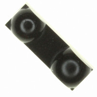
TFBS4711-TT1
Manufacturer Part Number
TFBS4711-TT1
Description
IRDA TRANSCEIVER SIR SV-e4
Manufacturer
Vishay
Type
TX/RXr
Specifications of TFBS4711-TT1
Peak Wavelength
900nm
Angle Of Half Sensitivity
44°
Pulse Width
2us
Communication Distance
100
Led Supply Voltage
-0.5 to 6V
Package Type
SMD
Fall Time
100ns
Rise Time
100ns
Dimensions
6x3.1x1.9
Operating Supply Voltage (typ)
2.5/3.3/5V
Operating Supply Voltage (min)
2.4V
Operating Supply Voltage (max)
5.5V
Mounting
Surface Mount
Pin Count
6
Operating Temp Range
-25C to 85C
Operating Temperature Classification
Commercial
Data Rate
115.2Kbps
Idle Current, Typ @ 25° C
75µA
Link Range, Low Power
1m
Operating Temperature
-30°C ~ 85°C
Orientation
Top View
Shutdown
*
Size
6mm x 3.1mm x 1.9mm
Standards
IrPHY 1.2
Supply Voltage
2.7 V ~ 5.5 V
Lead Free Status / RoHS Status
Compliant
Lead Free Status / RoHS Status
Compliant
Available stocks
Company
Part Number
Manufacturer
Quantity
Price

Part Number:
TFBS4711-TT1
Manufacturer:
VISHAY/威世
Quantity:
20 000


TFBS4711
Vishay Semiconductors
Optoelectronic Characteristics
Receiver
T
**)
tion while the source is operating at the minimum intensity in angular range into the minimum half-angle range at the maximum Link Length.
***)
maximum intensity in angular range at Minimum Link Length must not cause receiver overdrive distortion and possible related link errors.
If placed at the Active Output Interface reference plane of the transmitter, the receiver must meet its bit error ratio (BER).
For more definitions see the document “Symbols and Terminology” on the Vishay Website (http://www.vishay.com/docs/82512/82512.pdf).
Transmitter
T
www.vishay.com
4
Minimum irradiance E
angular range **)
Maximum irradiance E
angular range***)
Maximum no detection
irradiance
Rise time of output signal
Fall time of output signal
RXD pulse width
Leading edge jitter
Standby /Shutdown delay,
receiver startup time
Latency
IRED operating current
Transceiver operating peak
supply current
IRED leakage current
Output radiant intensity
Output radiant intensity, angle of
half intensity
Peak-emission wavelength
Spectral bandwidth
Optical rise time
Optical fall time
Optical output pulse duration
Optical overshoot
amb
amb
IrDA sensitivity definition: Minimum Irradiance E
Maximum Irradiance E
= 25 °C, V
= 25 °C, V
Parameter
Parameter
CC
CC
= 2.4 V to 5.5 V unless otherwise noted
= 2.4 V to 5.5 V unless otherwise noted.
e
e
in
in
e
In Angular Range, power per unit area. The optical delivered to the detector by a source operating at the
9.6 kbit/s to 115.2 kbit/s
λ = 850 nm - 900 nm,
α = 0°, 15°
λ = 850 nm - 900 nm
10 % to 90 %, C
90 % to 10 %, C
Input pulse width > 1.2 µs
Input Irradiance = 100 mW/m
≤ 115.2 kbit/s
After shutdown active
or power-on
T
During pulsed IRED operation at
I
TXD = 0 V, 0 < V
α = 0°, TXD = High, SD = Low,
R = 0 Ω, V
α = 0°, 15°, TXD = High, SD =
Low, R = 0 Ω, V
V
High or SD = High (Receiver is
inactive as long as SD = High)
Input pulse width 1.63 µs,
115.2 kbit/s
Input pulse width t
Input pulse width t
D
amb
CC
= 300 mA
= 5.0 V, α = 0°, 15°, TXD =
= - 25 °C to + 85 °C
Test Conditions
Test Conditions
LED
= 2.4 V
LED
L
L
CC
e
= 15 pF
= 15 pF
TXD
TXD
In Angular Range, power per unit area. The receiver must meet the BER specifica-
< 5.5 V
= 2.4 V
< 20 µs
≥ 20 µs
2
,
Symbol
Symbol
t
t
r(RXD)
f(RXD)
I
t
t
IRED
t
I
t
t
t
E
E
E
Δλ
ropt
PW
λ
fopt
I
CC
opt
opt
opt
t
I
I
I
α
D
L
e
e
e
p
e
e
e
(0.4)
1.41
t
Min
Min
200
880
1.7
TXD
- 1
10
10
45
25
10
10
4
(500)
(3.5)
0.57
± 22
1.63
Typ.
Typ.
300
2.0
35
60
35
45
5
Document Number 82633
t
TXD
Max
Max
0.04
2.23
0.15
100
100
250
150
150
400
300
300
900
100
100
300
3.0
80
(8)
25
Rev. 1.9, 07-Nov-06
1
+
(mW/cm
(µW/cm
(µW/cm
mW/m
mW/m
kW/m
mW/sr
mW/sr
mW/sr
Unit
Unit
mA
mA
nm
nm
µA
ns
ns
µs
ns
µs
µs
ns
ns
µs
µs
µs
%
°
2
2
2
2
2
2
)
)
)
Related parts for TFBS4711-TT1
Image
Part Number
Description
Manufacturer
Datasheet
Request
R

Part Number:
Description:
Infrared Transceivers SIR 115.2 kbits/s 2.7-5.5V Op Voltage
Manufacturer:
Vishay
Datasheet:

Part Number:
Description:
IRDA TX/RX 0.1152Mbps 2.5V/3.3V/5V 6-Pin SMD T/R
Manufacturer:
Vishay
Datasheet:
Part Number:
Description:
Serial Infrared Transceiver Sir, 115.2 Kbit/s, 2.7 V To 5.5 V Operation
Manufacturer:
Vishay
Datasheet:
Part Number:
Description:
357-036-542-201 CARDEDGE 36POS DL .156 BLK LOPRO
Manufacturer:
Vishay
Datasheet:
Part Number:
Description:
357-036-542-201 CARDEDGE 36POS DL .156 BLK LOPRO
Manufacturer:
Vishay
Datasheet:
Part Number:
Description:
357-036-542-201 CARDEDGE 36POS DL .156 BLK LOPRO
Manufacturer:
Vishay
Datasheet:
Part Number:
Description:
357-036-542-201 CARDEDGE 36POS DL .156 BLK LOPRO
Manufacturer:
Vishay
Datasheet:
Part Number:
Description:
357-036-542-201 CARDEDGE 36POS DL .156 BLK LOPRO
Manufacturer:
Vishay
Datasheet:
Part Number:
Description:
357-036-542-201 CARDEDGE 36POS DL .156 BLK LOPRO
Manufacturer:
Vishay
Datasheet:
Part Number:
Description:
357-036-542-201 CARDEDGE 36POS DL .156 BLK LOPRO
Manufacturer:
Vishay
Datasheet:
Part Number:
Description:
357-036-542-201 CARDEDGE 36POS DL .156 BLK LOPRO
Manufacturer:
Vishay
Datasheet:
Part Number:
Description:
357-036-542-201 CARDEDGE 36POS DL .156 BLK LOPRO
Manufacturer:
Vishay
Datasheet:
Part Number:
Description:
357-036-542-201 CARDEDGE 36POS DL .156 BLK LOPRO
Manufacturer:
Vishay
Datasheet:
Part Number:
Description:
357-036-542-201 CARDEDGE 36POS DL .156 BLK LOPRO
Manufacturer:
Vishay
Datasheet:
Part Number:
Description:
357-036-542-201 CARDEDGE 36POS DL .156 BLK LOPRO
Manufacturer:
Vishay
Datasheet: