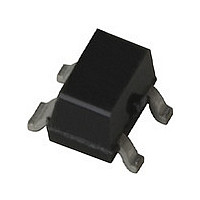
ATF-38143-TR2 Avago Technologies US Inc., ATF-38143-TR2 Datasheet - Page 4

ATF-38143-TR2
Manufacturer Part Number
ATF-38143-TR2
Description
TRANSISTOR,HEMT,N-CHAN,4.5V V(BR)DSS,90mA I(DSS),SOT-343R
Manufacturer
Avago Technologies US Inc.
Datasheet
1.ATF-38143-TR2.pdf
(13 pages)
Specifications of ATF-38143-TR2
Channel Type
N
Configuration
Single Dual Source
Gate-source Voltage (max)
4V
Operating Temperature Classification
Military
Mounting
Surface Mount
Package Type
SOT-343
Lead Free Status / RoHS Status
Contains lead / RoHS non-compliant
Available stocks
Company
Part Number
Manufacturer
Quantity
Price
Part Number:
ATF-38143-TR2G
Manufacturer:
AVAGO/安华高
Quantity:
20 000
ATF-38143 Typical Performance Curves
Notes:
1. Measurements made on a fixed tuned production test board that was tuned for optimal gain match with reasonable noise figure at 2 V 10 mA
2. P
4
Figure 6. OIP3 and P
Figure 9. Noise Figure vs. I
0.7
0.6
0.5
0.4
0.3
0.2
0.1
bias. This circuit represents a trade-off between an optimal noise match, maximum gain match and a realizable match based on production test
board requirements. Circuit losses have been de-embedded from actual measurements.
drain current may increase or decrease depending on frequency and dc bias point. At lower values of I
as power output approaches P
by a constant current source as is typically done with active biasing.
30
25
20
15
10
5
0
0
1dB
0
0
measurements are performed with passive biasing. Quiescent drain current, I
10
10
OIP3
CURRENT, I
CURRENT, I
20
20
1dB
vs. I
d
30
30
d
at 2V, 900 MHz.
P
at 2V, 2 GHz.
DS
1dB
DS
(mA)
(mA)
40
40
1dB
50
50
. This results in higher P
60
60
Figure 7. OIP3 and P
Figure 10. Associated Gain vs. I
30
25
20
15
10
22
21
20
19
18
17
16
15
5
0
0
0
1dB
and higher PAE (power added efficiency) when compared to a device that is driven
10
10
CURRENT, I
CURRENT, I
20
20
1dB
OIP3
vs. I
30
30
d
P
at 2V, 900 MHz.
DS
DS
1dB
d
at 2V, 2 GHz.
(mA)
(mA)
40
40
DSQ
50
, is set with zero RF drive applied. As P
50
60
60
Figure 11. Associated Gain vs. I
Figure 8. Noise Figure vs. I
DSQ
0.7
0.6
0.5
0.4
0.3
0.2
0.1
22
21
20
19
18
17
16
15
0
the device is running closer to class B
0
0
10
10
CURRENT, I
CURRENT, I
20
20
1dB
30
30
d
is approached, the
at 2V, 2 GHz.
DS
DS
d
at 2V, 900 MHz.
(mA)
(mA)
40
40
50
50
60
60


