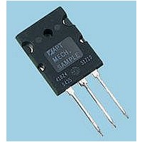
IXFK140N30P IXYS SEMICONDUCTOR, IXFK140N30P Datasheet

IXFK140N30P
Manufacturer Part Number
IXFK140N30P
Description
MOSFET, N, TO-264
Manufacturer
IXYS SEMICONDUCTOR
Datasheet
1.IXFK140N30P.pdf
(5 pages)
Specifications of IXFK140N30P
Transistor Polarity
N Channel
Continuous Drain Current Id
140A
Drain Source Voltage Vds
300V
On Resistance Rds(on)
24mohm
Rds(on) Test Voltage Vgs
10V
Voltage Vgs Max
20V
Operating Temperature Range
-55°C To
Threshold Voltage Vgs Typ
5V
Rohs Compliant
Yes
Lead Free Status / RoHS Status
Lead free / RoHS Compliant
Available stocks
Company
Part Number
Manufacturer
Quantity
Price
Company:
Part Number:
IXFK140N30P
Manufacturer:
ON
Quantity:
10 000
PolarHV
Power MOSFET
N-Channel Enhancement Mode
Avalanche Rated
Fast Intrinsic Diode
Symbol
V
V
V
V
I
I
I
I
E
E
dv/dt
P
T
T
T
T
T
F
M
Weight
Symbol
(T
BV
V
I
I
R
D25
L
DM
AR
GSS
DSS
© 2006 IXYS All rights reserved
J
JM
stg
L
DSS
DGR
GSM
GSM
AR
AS
D
SOLD
C
GS(th)
DS(on)
d
J
DSS
= 25° C unless otherwise specified)
Test Conditions
T
T
Transient
Continuous
T
Lead Current Limit, RMS
T
T
T
T
I
T
T
1.6 mm (0.062 in.) from case for 10 s
Plastic body for 10 seconds
Mounting force (PLUS247)
Mounting torque (TO-264)
TO-264
PLUS247
Test Conditions
V
V
V
V
V
S
V
J
J
C
C
C
C
C
J
C
GS
DS
GS
DS
GS
GS
= 25° C to 150° C
= 25° C to 150° C; R
= 25° C
= 25° C, pulse width limited by T
= 25° C
= 25° C
= 25° C
≤ I
≤ 150° C, R
= 25° C
TM
= 0 V, I
= V
= ± 20 V
= V
= 0 V
= 10 V, I
DM
, di/dt ≤ 100 A/µs, V
GS
DSS
HiPerFET
, I
D
D
DC
D
= 3 mA
= 8 mA
G
= 0.5 I
, V
= 2 Ω
DS
= 0
D25
GS
= 1 MΩ
DD
T
J
≤ V
= 125° C
DSS
IXFK 140N30P
IXFX 140N30P
JM
,
300
Min.
20..120/4.5..25
3.0
Characteristic Values
-55 ... +150
-55 ... +150
Maximum Ratings
Typ.
20
1.13/10 Nm/lb.in.
1040
± 30
± 20
300
300
140
300
150
300
260
75
80
80
20
10
± 200
5
6
Max.
5.0
25
24
1
V/ns
N/lb
mΩ
mA
mJ
nA
µA
°C
°C
°C
°C
°C
W
V
V
V
V
A
A
A
A
V
V
g
g
J
TO-264 (IXFK)
PLUS247 (IXFX)
Features
l
l
l
Advantages
l
l
l
International standard package
Unclamped Inductive Switching (UIS)
rated
Low package inductance
- easy to drive and to protect
Easy to mount
Space savings
High power density
V
I
R
t
D25
rr
G = Gate
D = Drain
DS(on)
DSS
G
D
D
S
S
≤ ≤ ≤ ≤ ≤ 24
≤ ≤ ≤ ≤ ≤ 200
= 300
= 140
S = Source
Tab = Collector
D (TAB)
DS99557E(03/06)
D (TAB)
mΩ Ω Ω Ω Ω
ns
A
V
Related parts for IXFK140N30P
IXFK140N30P Summary of contents
Page 1
PolarHV HiPerFET TM Power MOSFET N-Channel Enhancement Mode Avalanche Rated Fast Intrinsic Diode Symbol Test Conditions 25° 150° C DSS 25° 150° DGR J V Transient GSM ...
Page 2
Symbol Test Conditions 0 D25 C iss 500 kHz oss rss t d(on ...
Page 3
Fig. 1. Output Characteristics @ 25ºC 140 V = 10V GS 120 100 0 Volts DS Fig. 3. Output Characteristics @ 125ºC 140 V GS 120 100 80 60 ...
Page 4
Fig. 7. Input Admittance 180 160 140 120 100 T = 125º 25ºC - 40º 3 Volts GS Fig. 9. Forward Voltage Drop of Intrinsic Diode 300 250 200 ...
Page 5
IXYS All rights reserved Fig. 13. Maximum Transient Thermal Resistance 0.001 0.01 Pulse W idth - Seconds IXFK 140N30P IXFX 140N30P 0.1 1 IXYS REF: F_140N30P (93) 03-13-06.xls 10 ...


