GA300ABPL12 GeneSiC Semiconductor, GA300ABPL12 Datasheet
GA300ABPL12
Specifications of GA300ABPL12


Related parts for GA300ABPL12


GA300ABPL12 Summary of contents
Page 1
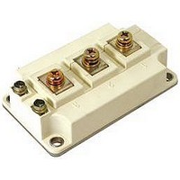
... Free-wheeling diode DC-Forward Current Repetitive Peak Forward Current Forward Surge Current Thermal Properties Th. Resistance Junction to Case Th. Resistance Case to Heat Sink Mechanical Properties Mounting Torque Terminal Connection Torque Weight Case Color Dimensions © 2010 GeneSiC Semiconductor Symbol Conditions V CES I T =25ºC (85º GES T ...
Page 2
Parameter IGBT Gate Threshold Voltage Collector-Emitter Cut-Off Current Gate-Leakage Current Collector-Emitter Threshold Voltage Collector-Emitter Slope Resistance Collector-Emitter Saturation Voltage Input Capacitance Output Capacitance Reverse Transfer Capacitance Stray Module Inductance Rise Time Fall Time Turn-On Energy Loss Per Pulse Turn-Off Energy ...
Page 3
... Figure 3: Typical Transfer Characteristics Figure 5: Typical Turn On Gate Charge Figure 7: Typical Turn Off Energy vs Collector Current © 2010 GeneSiC Semiconductor Figure 4: Typical FWD Forward Characteristics Figure 6: Typical Turn On Energy vs Collector Current Figure 8: Typical FWD Turn Off Characteristics Page http://www.genesicsemi.com ...
Page 4
... GeneSiC Semiconductor Page http://www.genesicsemi.com ...