VC060314A300TP AVX Corporation, VC060314A300TP Datasheet - Page 3
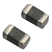
VC060314A300TP
Manufacturer Part Number
VC060314A300TP
Description
VARISTOR, 18.5V, 32V, 0603
Manufacturer
AVX Corporation
Series
VCr
Specifications of VC060314A300TP
Suppressor Type
Transient Voltage
Peak Surge Current @ 8/20µs
30A
Varistor Case
0603
Clamping Voltage Vc Max
32V
Peak Energy (10/1000us)
0.1J
Voltage Rating Vdc
14V
Voltage Rating Vac
10V
Product
MLV
Voltage Rating Dc
14 V
Capacitance
30 pF
Operating Temperature Range
- 55 C to + 125 C
Package / Case
0603 (1608 metric)
Lead Free Status / RoHS Status
Lead free / RoHS Compliant
Available stocks
Company
Part Number
Manufacturer
Quantity
Price
Company:

Part Number:
VC060314A300TP
Manufacturer:
AVX
Quantity:
400 000


AntennaGuard 0402/0603
AVX Multilayer Ceramic Transient Voltage Suppressors
ESD Protection for Antennas and Low Capacitor Loading Applications
Antenna Varistors
AVX offers a series of 0402 and 0603 chip varistors,
designated the AntennaGuard series, for RF antenna/RF
amplifier protection. These devices offer ultra-low capaci-
tance (<3pF in 0402 chips, and ≤3pF & ≤12pF in 0603
packages), as well as low insertion loss. Antenna varistors
can replace output capacitors and provide ESD suppression
in cell phones, pagers and wireless LANs.
It is very common to employ some form of a FET in many
types of efficient/miniature RF amplifiers. Typically, these RF
transistors have nearly ideal input gate impedance and
outstanding noise figures. However, FETs are very suscepti-
ble to ESD damage due to the very thin layer of SiO
the gate insulator. The ultra-thin SiO
improve the gain of the transistor. In other words, the upside
of the performance enhancement becomes the downside of
the transistors survival when subjected to an ESD event.
ESD damage to the RF Field Effect Transistors (FETs) is a
34
Suppression Device
AVX 0402 TransGuard
AVX 0603 TransGuard
Competitor’s SOT23 Diode
®
®
D1
Figure 1A. 0402/0603
IR Solder Pad Layout
D2
D3
D4
1.70 (0.067)
2.54 (0.100)
2
D5
D1
layer is required to
2
uses as
0.61 (0.024)
0.89 (0.035)
D2
growing concern among RF designers due to the following
trends: (1) RF amplifiers continue to shrink in size, and (2)
FET gains figures continue to increase. Both trends relate to
decreasing gate oxide thickness, which in turn, is directly
proportional to increased ESD sensitivity. As miniaturization
trends accelerate, the traditional methods to protect against
ESD damage (i.e., PC board layout, passive filters, and diode
clamps) are becoming less and less effective.
AVX’s AntennaGuard varistor can be used to protect the FET
and offer superior performance to the previously mentioned
protection methods given above. The standard EIA 0603
chip size, and particularly the 0402 chip, offer designers an
ESD protection solution consistent with today’s downsizing
trend in portable electronic products. Savings in component
volume up to 86%, and PC board footprint savings up to
83% are realistic expectations. These percentages are based
upon the following table and Figures 1A and 1B.
Pad Dimensions
0.51 (0.020)
0.76 (0.030)
(0.035)
Figure 1B. SOT23- Solder Pad Layout
See Below
0.9
D3
(0.037)
0.96
(0.037)
0.96
(0.031)
0.8
0.61 (0.024)
0.89 (0.035)
(0.079)
2.0
D4
mm (inch
mm (inches)
0.51 (0.020)
0.76 (0.030)
D5
Related parts for VC060314A300TP
Image
Part Number
Description
Manufacturer
Datasheet
Request
R

Part Number:
Description:
Manufacturer:
AVX Corporation
Datasheet:
Part Number:
Description:
Manufacturer:
AVX Corporation
Datasheet:
Part Number:
Description:
Manufacturer:
AVX Corporation
Datasheet:
Part Number:
Description:
Manufacturer:
AVX Corporation
Datasheet:
Part Number:
Description:
Manufacturer:
AVX Corporation
Datasheet: