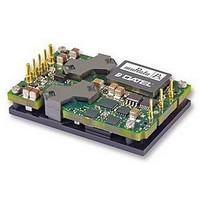
UQQ-5/20-Q48P-C Murata Power Solutions Inc, UQQ-5/20-Q48P-C Datasheet - Page 6
UQQ-5/20-Q48P-C
Manufacturer Part Number
UQQ-5/20-Q48P-C
Description
CONVERTER, DC/DC, WI, 100W, 5V
Manufacturer
Murata Power Solutions Inc
Series
UQQr
Datasheet
1.UQQ-3.325-Q12P-C.pdf
(14 pages)
Specifications of UQQ-5/20-Q48P-C
Output Type
Single
No. Of Output Channels
1
Input Voltage
18V To 75V
Power Rating
100W
Output Voltage
5V
Output Current
20A
Supply Voltage
48V
Dc / Dc Converter Case Style
Quarter Brick
Dc / Dc Converter O/p Type
Single
No. Of Outputs
1
Approval Bodies
EN / IEC / UL
Rohs Compliant
Yes
Product
Isolated
Output Power
100 W
Input Voltage Range
18 V to 75 V
Input Voltage (nominal)
48 V
Number Of Outputs
1
Output Voltage (channel 1)
5 V
Output Current (channel 1)
20 A
Isolation Voltage
2.25 KV
Package / Case Size
Quarter Brick
Lead Free Status / RoHS Status
Lead free / RoHS Compliant


www.cd4power.com
Removal of Soldered UQQ's from Printed Circuit Boards
Should removal of the UQQ from its soldered connection be needed, thor-
oughly de-solder the pins using solder wicks or de-soldering tools. At no
time should any prying or leverage be used to remove boards that have not
been properly de-soldered first.
Input Source Impedance
UQQ converters must be driven from a low ac-impedance input source.
The DC/DC’s performance and stability can be compromised by the use of
highly inductive source impedances. The input circuit shown in Figure 2
is a practical solution that can be used to minimize the effects of induct-
ance in the input traces. For optimum performance, components should be
mounted close to the DC/DC converter.
I/O Filtering, Input Ripple Current, and Output Noise
All models in the UQQ Series are tested/specified for input ripple cur-
rent (also called input reflected ripple current) and output noise using the
circuits and layout shown in Figures 2 and 3.
P O W E R E L E C T R O N I C S D I V I S I O N
Absolute Maximum Ratings
Input Voltage
On/Off Control
Input Reverse Polarity Protection
Output Overvoltage
Output Current
Absolute maximums are stress ratings. Exposure of devices to any of these
conditions may adversely affect long-term reliability. Proper operation under
conditions other than those listed in the Performance/Functional Specifications
Table is not implied nor recommended.
T E C H N I C A L N O T E S
Storage Temperature
Lead Temperature (soldering 0 sec. max.) +280
Continuous
Transient (00msec)
V
OSCILLOSCOPE
IN
+
–
C
C
L
TO
BUS
IN
BUS
= 33µF, ESR < 700mΩ @ 100kHz
= 12µH
= 220µF, ESR < 100mΩ @ 100kHz
(7)
Figure 2. Measuring Input Ripple Current
C
BUS
L
BUS
12V models
0 to +36V
+50V
CURRENT
PROBE
C
IN
0V min to +3.5V max.
See Fuse section
V
Current-limited. Devices can
withstand sustained short circuit
without damage.
–55 to +25
OUT
3
1
+20% max.
°
C
+INPUT
–INPUT
48V models
0 to +75V
°
+00V
C
External input capacitors (C
age elements. They should be selected for bulk capacitance (at appropriate
frequencies), low ESR, and high rms-ripple-current ratings. The switching
nature of DC/DC converters requires that dc voltage sources have low ac
impedance as highly inductive source impedance can affect system stabil-
ity. In Figure 2, C
system configuration may necessitate additional considerations.
In critical applications, output ripple/noise (also referred to as periodic and
random deviations or PARD) can be reduced below specified limits using
filtering techniques, the simplest of which is the installation of additional
external output capacitors. Output capacitors function as true filter
elements and should be selected for bulk capacitance, low ESR, and
appropriate frequency response. In Figure 3, the two copper strips simulate
real-world pcb impedances between the power supply and its load. Scope
measurements should be made using BNC connectors or the probe ground
should be less than ½ inch and soldered directly to the fixture.
All external capacitors should have appropriate voltage ratings and be
located as close to the converter as possible. Temperature variations for all
relevant parameters should be taken into consideration. OS-CON
semiconductor capacitors (www.sanyo.com) can be especially effective for
further reduction of ripple/noise.
The most effective combination of external I/O capacitors will be a function
of line voltage and source impedance, as well as particular load and layout
conditions. Our Applications Engineers can recommend potential solutions
and discuss the possibility of our modifying a given device’s internal filter-
ing to meet your specific requirements. Contact our Applications Engineer-
ing Group for additional details.
+OUTPUT
–OUTPUT
+SENSE
–SENSE
Figure 3. Measuring Output Ripple/Noise (PARD)
Wide Input Range Single Output DC/DC Converters
BUS
and L
C1 = 1µF CERAMIC
C2 = 10µF TANTALUM
LOAD 2-3 INCHES (51-76mm) FROM MODULE
7
8
4
5
BUS
IN
C1
simulate a typical dc voltage bus. Your specific
in Figure 2) serve primarily as energy-stor-
COPPER STRIP
COPPER STRIP
C2
D C / D C C O N V E R T E R S
SCOPE
UQQ Series
MDC_UQQ_A02
R
TM
LOAD
organic
Page 6 of 4
Related parts for UQQ-5/20-Q48P-C
Image
Part Number
Description
Manufacturer
Datasheet
Request
R

Part Number:
Description:
CONV DC/DC 100W 20A 5V T/H
Manufacturer:
Murata Power Solutions Inc
Datasheet:

Part Number:
Description:
DC/DC Converter
Manufacturer:
Murata Power Solutions Inc
Datasheet:

Part Number:
Description:
DC/DC Converters & Regulators 48Vin 5Vout 20A neg polarity TH
Manufacturer:
Murata Power Solutions Inc
Datasheet:
Part Number:
Description:
CONV DC/DC 85W 17A 5V T/H
Manufacturer:
Murata Power Solutions Inc
Datasheet:
Part Number:
Description:
DC/DC TH 17A 12-5V Q-brick
Manufacturer:
Murata Power Solutions Inc

Part Number:
Description:
DC/DC Converter
Manufacturer:
Murata Power Solutions Inc
Datasheet:

Part Number:
Description:
DC/DC TH 17A 12-5V Q-brick
Manufacturer:
Murata Power Solutions Inc
Part Number:
Description:
CONV DC/DC 82.5W 25A 3.3V T/H
Manufacturer:
Murata Power Solutions Inc
Datasheet:

Part Number:
Description:
CONV DC/DC 96W 8A 12V T/H
Manufacturer:
Murata Power Solutions Inc
Datasheet:
Part Number:
Description:
CONV DC/DC 96W 4A 24V T/H
Manufacturer:
Murata Power Solutions Inc
Datasheet:
Part Number:
Description:
CONV DC/DC 85W 17A 5V T/H
Manufacturer:
Murata Power Solutions Inc
Datasheet:

Part Number:
Description:
Transformers 5Vin 5Vout 200mA 4000Vdc 1:1.33 turn
Manufacturer:
Murata Power Solutions Inc
Datasheet:
Part Number:
Description:
POWER SUPPLY
Manufacturer:
Murata Power Solutions Inc
Datasheet:

Part Number:
Description:
DPM LED MINI 2VDC 3.5DIG LP RED
Manufacturer:
Murata Power Solutions Inc
Datasheet:

Part Number:
Description:
CONV DC/DC 1W 5VIN 5VOUT SIP SGL
Manufacturer:
Murata Power Solutions Inc
Datasheet: