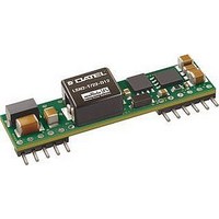
LSN2-T/10-D12NG-C Murata Power Solutions Inc, LSN2-T/10-D12NG-C Datasheet - Page 11

LSN2-T/10-D12NG-C
Manufacturer Part Number
LSN2-T/10-D12NG-C
Description
DC/DC Converter
Manufacturer
Murata Power Solutions Inc
Datasheet
1.LSN2-T10-D12G-C.pdf
(15 pages)
Specifications of LSN2-T/10-D12NG-C
No. Of Outputs
1
Input Voltage
8.3V To 14V
Power Rating
50W
Output Current
10A
Approval Bodies
UL, CSA
Supply Voltage
14VDC
Dc / Dc Converter Case Style
SIP
Dc/dc Converter Mounting
Through Hole
Product
Non-Isolated / POL
Output Power
50 W
Input Voltage Range
8.3 V to 14 V
Number Of Outputs
1
Output Voltage (channel 1)
1.75 V to 5 V
Output Current (channel 1)
10 A
Package / Case Size
SIP
Lead Free Status / RoHS Status
Lead free / RoHS Compliant
other method. Several standard sequencing architectures are prevalent. They
are concerned with three factors:
difference relationship is important for systems very concerned about possible
latchup of programmable devices or overdriving ESD diodes. Lower slew
rates avoid overcurrent shutdown during bypass cap charge-up.
ferent respective fi nal set point voltages. During the ramp, their voltages are
nearly identical. This avoids problems with large currents fl owing between
logic systems which are not initialized yet. Since both end voltages are differ-
ent, each converter reaches it’s setpoint voltage at a different time.
fi nal voltages at about the same time.
■
■
■
For most systems, the time relationship is the dominant factor. The voltage
In Figure 8, two POL’s ramp up at the same rate until they reach their dif-
Figure 9 shows two POLs with different slew rates in order to reach differing
The time relationship between the Master and Slave voltages
The voltage difference relationship between the Master and Slave
The voltage slew rate (ramp slope) of each converter’s output.
Figure 8. Coincident or Simultaneous Phasing (Identical Slew Rates)
Figure 9. Proportional or Ratiometric Phasing (Identical V
OUT
Time)
www.murata-ps.com
for two converters. Figure 10 is called “Inclusive” because the later starting
POL fi nishes inside the earlier POL. The timing in Figure 10 is more easily built
using a combined digital sequence controller and the Sequence/Track pin.
relationship staggered approximately the same at power-up and power-down.
Operation
To use the Sequence pin after power start-up stabilizes, apply a rising external
voltage to the Sequence input. As the voltage rises, the output voltage will
track the Sequence input (gain = 1). The output voltage will stop rising when
it reaches the normal set point for the converter. The Sequence input may op-
tionally continue to rise without any effect on the output. Keep the Sequence
input voltage below the converter’s input supply voltage.
until the Sequence input falls below the set point.
below show simple RC networks but you may also use operational amplifi ers,
D/A converters, etc.
Figure 11. Staggered or Sequential Phasing—Exclusive (Fixed Cascaded Delays)
Figures 10 and 11 show both delayed start up and delayed fi nal voltages
Figure 11 is the same strategy as Figure 10 but with an “exclusive” timing
Use a similar strategy on power down. The output voltage will stay constant
Any strategy may be used to deliver the power up/down ramps. The circuits
Figure 10. Staggered or Sequential Phasing—Inclusive (Fixed Delays)
Selectable-Output DC/DC Converters
25 Jun 2010
Non-isolated, DOSA-SIP, 6/10/16A
LSN2 Series
MDC_LSN2.B07Δ
email: sales@murata-ps.com
Page 11 of 15


