LSM-1.8/10-D3-C Murata Power Solutions Inc, LSM-1.8/10-D3-C Datasheet - Page 3
LSM-1.8/10-D3-C
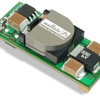
Manufacturer Part Number
LSM-1.8/10-D3-C
Description
DC/DC SM 10A 3-1.8V Non-Iso
Manufacturer
Murata Power Solutions Inc
Series
LSMr
Datasheet
1.LSM-0.810-D3-C.pdf
(13 pages)
Specifications of LSM-1.8/10-D3-C
Product
Non-Isolated / POL
Output Power
18 W
Input Voltage Range
3 V to 3.6 V
Number Of Outputs
1
Output Voltage (channel 1)
1.8 V
Output Current (channel 1)
10 A
Output Type
Low Voltage
Lead Free Status / Rohs Status
Lead free / RoHS Compliant


Performance/Functional Specifications
Typical @ T
Input Voltage Range
Input Current:
Input Reflected Ripple Current
Input Filter Type
Overvoltage Protection
Reverse-Polarity Protection
Undervoltage Shutdown
On/Off Control
V
Minimum Loading
Maximum Capacitive Load
V
Ripple/Noise (20MHz BW)
Total Accuracy
Efficiency
Overcurrent Detection and Short-Circuit Protection:
Transient Response (50% load step)
Start-Up Time:
Switching Frequency:
Calculated MTBF
Operating Temperature: (Ambient)
With Derating
Thermal Shutdown
Dimensions
Pin Dimensions/Material
Weight
Flammability Rating
Safety
OUT
OUT
Normal Operating Conditions
Inrush Transient
Standby/Off Mode
Output Short-Circuit Condition
Current-Limiting Detection Point
Short-Circuit Detection Point
SC Protection Technique
Short-Circuit Current
V
Without Derating (Natural convection) –40 to +65/71°C (model dependent)
On/Off to V
See Technical Notes and Performance Curves for details.
All models are tested and specified with external 22μF tantalum input and output capacitors.
These capacitors are necessary to accommodate our test equipment and may not be
required to achieve specified performance in your applications. All models are stable and
regulate within spec under no-load conditions.
The On/Off Control (pin 1) is designed to be driven with open-collector logic or the appli-
cation of appropriate voltages (referenced to Common, pin 3). Applying a voltage to On/Off
Control when no input voltage is applied to the converter may cause permanent damage.
Output noise may be further reduced with the installation of additional external output
filtering. See I/O Filtering and Noise Reduction.
MTBF’s are calculated using Telcordia SR-332(Bellcore), ground fixed, T
power, natural convection, +67°C pcb temperature.
IN
Trim Range
to V
Accuracy (50% load)
A
OUT
= +25°C under nominal line voltage and full-load conditions unless noted.
OUT
Dynamic Characteristics
Environmental
Physical
Output
Input
4.5 to 5.5 Volts (5V nominal)
See Ordering Guide
0.01A
8mA
110mA average
10mAp-p
Capacitive (44μF)
None
None
None
On = open (internal pull-up to +V
Off = 0 to +0.8V (1ma max.)
±1% maximum
No load
1000μF (low ESR, OSCON)
±10% (0.8V not trimmable)
See Ordering Guide
3% over line/load temperature
See Ordering Guide
17 (13-23.5) Amps
98% of V
Hiccup with auto recovery
600mA average
100μsec to ±2% of final value
7msec
6msec
300kHz (+40/–50kHz)
2.3 -1.8 million hours (1V
See Derating Curves
+115°C (110 to 125°C)
1.3" x 0.53" x 0.34" (33.02 x 13.46 x 8.64 mm)
0.112" x 0.062" (2.84 x 1.57mm) rectangular
copper with gold plate over nickel underplate
0.28 ounces (7.8g)
UL94V-0
UL/cUL/IEC/EN 60950,
CSA-C22.2 No. 60950
2
www.murata-ps.com
sec
OUT
set
OUT
A
to 5V
= +25°C, full
IN
OUT
)
)
I/O Filtering and Noise Reduction
All models in the LSM D3 Series are tested and specified with external
22μF tantalum input and output capacitors. These capacitors are necessary
to accommodate our test equipment and may not be required to achieve
desired performance in your application. The LSM D3's are designed with
high-quality, high-performance internal I/O caps, and will operate within spec
in most applications with no additional external components.
In particular, the LSM D3's input capacitors are specified for low ESR
and are fully rated to handle the units' input ripple currents. Similarly, the
internal output capacitors are specified for low ESR and full-range frequency
response. As shown in the Performance Curves, removal of the external
22μF tantalum output caps has minimal effect on output noise.
In critical applications, input/output ripple/noise may be further reduced using
filtering techniques, the simplest being the installation of external I/O caps.
External input capacitors serve primarily as energy-storage devices. They
minimize high-frequency variations in input voltage (usually caused by IR
drops in conductors leading to the DC/DC) as the switching converter draws
pulses of current. Input capacitors should be selected for bulk capacitance
(at appropriate frequencies), low ESR, and high rms-ripple-current ratings.
The switching nature of modern DC/DC's requires that the dc input voltage
source have low ac impedance at the frequencies of interest. Highly induc-
tive source impedances can greatly affect system stability. Your specific
system configuration may necessitate additional considerations.
Input Voltage:
On/Off Control (Pin 1)
Input Reverse-Polarity Protection
Output Overvoltage Protection
Output Current
short
without damage.
Storage Temperature
Lead Temperature (soldering, 10 sec.)
These are stress ratings. Exposure of devices to any of these conditions may adversely
affect long-term reliability. Proper operation under conditions other than those listed in the
Performance/Functional Specifications Table is not implied.
T E C H N I C A L
Continuous or transient
Single Output, Non-Isolated, 3.3V
Figure 2. Measuring Input Ripple Current
Technical enquiries email: sales@murata-ps.com, tel:
N O T E S
Absolute Maximum Ratings
LSM-10A D3 Models
10 Amp DC/DC’s in SMT Packages
6 Volts
+V
None
None
Current limited. Devices can
–40 to +125°C
See Reflow Solder Profile
IN
MDC_LSM-10A D3.B01 Page 3 of 13
withstand sustained output
circuits
IN
, 0.8-2.5V
+1 508 339 3000
OUT
Related parts for LSM-1.8/10-D3-C
Image
Part Number
Description
Manufacturer
Datasheet
Request
R

Part Number:
Description:
DC/DC SM 10A 12-1.8V Non-Iso
Manufacturer:
Murata Power Solutions Inc
Part Number:
Description:
DC/DC SM 10A 5-1.8V Non-Iso
Manufacturer:
Murata Power Solutions Inc
Part Number:
Description:
DC/DC SM 16A 12-1.8V Non-Iso
Manufacturer:
Murata Power Solutions Inc
Part Number:
Description:
DC/DC SM 16A W3-1.8V Non-Iso
Manufacturer:
Murata Power Solutions Inc
Datasheet:

Part Number:
Description:
DC/DC SM,10A,12-1.8V,NON-ISO
Manufacturer:
Murata Power Solutions Inc

Part Number:
Description:
POWER OVER ETHERNET MODULE
Manufacturer:
Murata Power Solutions Inc
Datasheet:

Part Number:
Description:
POWER OVER ETHERNET MODULE
Manufacturer:
Murata Power Solutions Inc
Datasheet:

Part Number:
Description:
POWER OVER ETHERNET MODULE
Manufacturer:
Murata Power Solutions Inc
Datasheet:

Part Number:
Description:
POWER OVER ETHERNET MODULE
Manufacturer:
Murata Power Solutions Inc
Datasheet:

Part Number:
Description:
Power Inductors 2.2mH1.4A
Manufacturer:
Murata Power Solutions Inc
Datasheet:

Part Number:
Description:
DC/DC Converter
Manufacturer:
Murata Power Solutions Inc
Datasheet:

Part Number:
Description:
Transformers 5Vin 5Vout 200mA 4000Vdc 1:1.33 turn
Manufacturer:
Murata Power Solutions Inc
Datasheet:
Part Number:
Description:
POWER SUPPLY
Manufacturer:
Murata Power Solutions Inc
Datasheet:

Part Number:
Description:
DPM LED MINI 2VDC 3.5DIG LP RED
Manufacturer:
Murata Power Solutions Inc
Datasheet:

Part Number:
Description:
CONV DC/DC 1W 5VIN 5VOUT SIP SGL
Manufacturer:
Murata Power Solutions Inc
Datasheet: