PRL-350ECL PULSE RESEARCH LAB, PRL-350ECL Datasheet - Page 2
PRL-350ECL
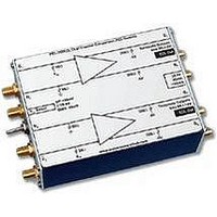
Manufacturer Part Number
PRL-350ECL
Description
Product Description:2-Ch. Comparator/Sinewave Converter, ECL Outputs
Manufacturer
PULSE RESEARCH LAB
Datasheet
1.PRL-350ECL.pdf
(2 pages)
Specifications of PRL-350ECL
Rohs Compliant
NA
Lead Free Status / RoHS Status
na


SPECIFICATIONS
Unless otherwise specified, dynamic measurements are made with all outputs terminated into 50 Ω/V
ECL outputs and 0 V for TTL outputs.
(1) If the switch is set to the center position (0 V threshold) a non-driven channel will oscillate and induce jitter in the driven channel. Connect any output to any
input to stop the oscillation.
(2) 20%-80% for ECL outputs, 10%-90% for TTL outputs. For the PRL-350ECL, an unused complementary output must be either terminated into 50 Ω/V
AC coupled into a 50 Ω load; otherwise, output waveform distortion and rise time degradation will occur. Use the PRL-ACT-50, Dual Channel AC-Coupled
50 Ω Termination, for terminating unused complementary outputs. Use the PRL-550NQ/PQ4X, Four Channel NECL/PECL Terminators, respectively, for the
50 Ω/V
0.1 µf DC block or the PRL-ACX-12dB, 12 dB AC-coupled attenuator may be used to connect the NECL/PECL outputs to 50 Ω input instruments.
For the PRL-350TTL, very slight output waveform distortion and rise time degradation will occur when an unused complementary output is not terminated. For
optimum performance, however, all outputs should be terminated.
(3) In order to reduce jitter near f
(4) Although the PRL-350ECL typically operates up to 2 GHz, the internal device is specified at 1 GHz by the device manufacturer; therefore the guaranteed
f
MAX
is 1 GHz.
SYMBOL
V
t SKEW
V
V
TT
NIM+
NIM-
t PLH
t PHL
V DC
V AC
R out
V
V
IN
f
V
V
V
I DC
V
IN
R in
t
IN
MAX
termination and for connection of NECL/PECL signals to 50 Ω input oscilloscopes. If preservation of DC levels is not required, then the PRL-SC-104,
r
TH+
TH0
TH-
CM
OL
OH
/t
II**
I**
III
f
Fig. 1A PRL-350ECL Block Diagram
Input Resistance
Output Resistance
Preset positive threshold voltage
Preset negative threshold voltage
Preset zero threshold voltage
Output Low Level
Output High Level
DC Input Current
DC Input Voltage
AC/DC Adapter Input Voltage
Propagation Delay to output ↑
Propagation Delay to output ↓
Rise/Fall Times
Skew between any 2 outputs
Minimum Input Voltage @ 150MHz
Minimum Input Voltage @ 250MHz
Minimum Input Voltage @ 1GHz
Input Common Mode Range
Max Clock Frequency
Size
Weight
MAX
PARAMETER
(0 o C ≤ T
, terminate the non-driven input into 50 Ω when the input voltage is less than 20 mV
(2)
(4)
A
≤ 35 o C)
(1)
(3)
(3)
1000
-404
Min
49.5
±7.5
396
103
250
-55
45
20
20
-2
-2
-1
PRL-350ECL
1.3 x 2.9 x 3.9
NPN emitter
-2.0/+3.0
36/ -136
2000
-400
±8.5
Typ
400
-1.6
-0.8
115
750
100
100
-50
1.5
1.5
50
10
10
0
0
7
45/-145
Max
-396
50.5
-1.5
-0.6
±12
Fig. 1B PRL-350TTL Block Diagram
404
127
850
300
-45
55
2
Min
49.5
49.5
-404
±7.5
396
-0.5
103
250
-55
45
20
40
-2
2
1234 Francisco Street, Torrance, CA 90502
Tel: 310-515-5330 Fax: 310-515-0068
PRL-350TTL
1.3 x 2.9 x 3.9
300/-285
-2.0/+3.0
1100
P-P
-400
±8.5
Typ
400
115
200
300
NA
-50
2.2
50
50
50
10
20
0
0
2
2
.
7
TT
sales@pulseresearchlab.com
, where V
www.pulseresearchlab.com
Document modified 10/25/07
325/-300
1250
Max
50.5
50.5
-396
404
±12
127
400
-45
0.5
2.4
55
2
TT
= -2 V for
mVp-p
mVp-p
mVp-p
UNIT
MHz
mV
mV
mV
mA
Oz
in.
ns
ns
ps
ps
Ω
Ω
V
V
V
V
V
TT
or
Related parts for PRL-350ECL
Image
Part Number
Description
Manufacturer
Datasheet
Request
R

Part Number:
Description:
Product Description:1:4TTLFanout Line Driver
Manufacturer:
PULSE RESEARCH LAB
Datasheet:

Part Number:
Description:
Universal Pi Network Kit, BNC M/F
Manufacturer:
PULSE RESEARCH LAB

Part Number:
Description:
Product Description:TTLFreq.Divider(f/2,f/4,f/8,f/16)
Manufacturer:
PULSE RESEARCH LAB
Datasheet:

Part Number:
Description:
Product Description:TTLFreq.Divider(f/2,f/10)
Manufacturer:
PULSE RESEARCH LAB
Datasheet:

Part Number:
Description:
Product Description:SmallSignalFreq.Divider(f/2,f/4)
Manufacturer:
PULSE RESEARCH LAB
Datasheet:

Part Number:
Description:
Product Description:NECLFreq.Divider(f/2,f/4),SMAI/O
Manufacturer:
PULSE RESEARCH LAB
Datasheet:

Part Number:
Description:
Product Description:PECLFreq.Divider(f/2,f/4),SMAI/O
Manufacturer:
PULSE RESEARCH LAB
Datasheet:

Part Number:
Description:
Product Description:ProgrammableNECL/TTLFrequencyDivider(f/2 - F/512)
Manufacturer:
PULSE RESEARCH LAB
Datasheet:

Part Number:
Description:
Product Description:2-Ch.Comparator/Sinewave Converter, TTL Outputs
Manufacturer:
PULSE RESEARCH LAB
Datasheet:

Part Number:
Description:
Product Description:2-Ch.Translator,TTLto NECL
Manufacturer:
PULSE RESEARCH LAB
Datasheet:

Part Number:
Description:
Product Description:2-Ch.Translator,TTLtoPECL
Manufacturer:
PULSE RESEARCH LAB
Datasheet:

Part Number:
Description:
Product Description:2-Ch.Translator,TTLtoDifferentialTTL
Manufacturer:
PULSE RESEARCH LAB
Datasheet:

Part Number:
Description:
Product Description:2-Ch.Translator,RS-422to NECL
Manufacturer:
PULSE RESEARCH LAB
Datasheet:

Part Number:
Description:
Product Description:2-Ch.Translator, NECLtoRS-422
Manufacturer:
PULSE RESEARCH LAB
Datasheet:
