SM72501/NOPB National Semiconductor, SM72501/NOPB Datasheet - Page 4
SM72501/NOPB
Manufacturer Part Number
SM72501/NOPB
Description
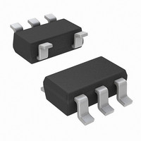
IC AMP CMOS INPUT SOT-23-5
Manufacturer
National Semiconductor
Series
SolarMagic™r
Datasheet
1.SM72501XNOPB.pdf
(20 pages)
Specifications of SM72501/NOPB
Amplifier Type
General Purpose
Number Of Circuits
1
Output Type
Rail-to-Rail
Slew Rate
1.1 V/µs
Gain Bandwidth Product
2.5MHz
Current - Input Bias
200nA
Voltage - Input Offset
37µV
Current - Supply
790µA
Current - Output / Channel
86mA
Voltage - Supply, Single/dual (±)
2.7 V ~ 12 V
Operating Temperature
-40°C ~ 125°C
Mounting Type
Surface Mount
Package / Case
*
Lead Free Status / RoHS Status
Lead free / RoHS Compliant
-3db Bandwidth
-


www.national.com
V
TCV
I
I
CMRR
PSRR
CMVR
A
V
I
I
SR
GBW
THD+N
e
i
n
B
OS
OUT
S
Symbol
n
OS
VOL
OUT
±5V Electrical Characteristics
Unless otherwise specified, all limits are guaranteed for T
face limits apply at the temperature extremes.
Note 1: Absolute Maximum Ratings indicate limits beyond which damage to the device may occur. Operating Ratings indicate conditions for which the device is
intended to be functional, but specific performance is not guaranteed. For guaranteed specifications and the test conditions, see the Electrical Characteristics
Tables.
Note 2: Human Body Model, applicable std. MIL-STD-883, Method 3015.7. Machine Model, applicable std. JESD22-A115-A (ESD MM std. of JEDEC) Field-
Induced Charge-Device Model, applicable std. JESD22-C101-C (ESD FICDM std. of JEDEC).
Note 3: The maximum power dissipation is a function of T
P
Note 4: Electrical Table values apply only for factory testing conditions at the temperature indicated. Factory testing conditions result in very limited self-heating
of the device such that T
T
A
D
.
OS
= (T
J(MAX)
Input Offset Voltage
Input Offset Voltage Temperature Drift
Input Bias Current
Input Offset Current
Common Mode Rejection Ratio
Power Supply Rejection Ratio
Common Mode Voltage Range
Open Loop Voltage Gain
Output Voltage Swing High
Output Voltage Swing Low
Output Current
(Note
Supply Current
Slew Rate
Gain Bandwidth
Total Harmonic Distortion + Noise
Input Referred Voltage Noise Density
Input Referred Current Noise Density
– T
A
)/ θ
3,
JA
Note
. All numbers apply for packages soldered directly onto a PC Board.
J
(Note
= T
9)
A
Parameter
. No guarantee of parametric performance is indicated in the electrical tables under conditions of internal self-heating where T
10)
J(MAX)
(Note
(Note
−40°C
(Note
−40°C
−5V
2.7V
CMRR
CMRR
R
V
R
V
R
R
R
R
Sourcing V
V
Sinking V
V
A
10% to 90%
f = 1 kHz, A
f = 1 kHz
f = 100 kHz
, θ
(Note
O
O
IN
IN
V
L
L
L
L
L
L
JA
= 2 kΩ
= 10 kΩ
= 2 kΩ to 0V
= 10 kΩ to 0V
= 2 kΩ to 0V
= 10 kΩ to 0V
= +1, V
= −4.7V to 4.7V
= −4.8V to 4.8V
. The maximum allowable power dissipation at any ambient temperature is
= 100 mV
= −100 mV
≤
≤
A
7)
7,
7,
4)
≤
≤
V
V
≥
≥
= 25°C, V
CM
Note
Note
+
T
T
80 dB
78 dB
O
A
A
≤
O
O
= 0V
V
Conditions
≤
≤
≤
= 9 V
4
12V, V
= 0V
= 1, R
8)
8)
5V
85°C
125°C
+
PP
= 5V, V
O
L
= 10 kΩ
= 0V
−
= −5V, V
CM
(Note
−5.2
−5.2
Min
= 0V, and R
100
100
92
88
86
82
98
98
50
35
50
35
6)
(Note
0.790
±0.2
±0.2
0.02
Typ
±37
138
121
134
1.1
2.5
±1
40
98
90
40
90
40
86
84
L
9
1
> 10 kΩ to 0V. Bold-
5)
(Note
±200
±500
±400
Max
±50
150
170
100
130
150
5.2
5.2
1.1
1.3
±5
80
50
60
1
1
6)
from V
from V
nV/
fA/
Units
μV/°C
V/μs
MHz
mV
mV
mA
mA
μV
pA
dB
dB
dB
fA
%
V
J
>
+
–
Related parts for SM72501/NOPB
Image
Part Number
Description
Manufacturer
Datasheet
Request
R

Part Number:
Description:
National Semiconductor [8-Bit D/A Converter]
Manufacturer:
National Semiconductor
Datasheet:
Part Number:
Description:
National Semiconductor [Media Coprocessor]
Manufacturer:
National Semiconductor
Datasheet:
Part Number:
Description:
Digitally Controlled Tone and Volume Circuit with Stereo Audio Power Amplifier, Microphone Preamp Stage and National 3D Sound
Manufacturer:
National Semiconductor
Datasheet:
Part Number:
Description:
Digitally Controlled Tone and Volume Circuit with Stereo Audio Power Amplifier, Microphone Preamp Stage and National 3D Sound
Manufacturer:
National Semiconductor
Datasheet:
Part Number:
Description:
AC97 Rev 2 Codec with Sample Rate Conversion and National 3D Sound
Manufacturer:
National Semiconductor
Part Number:
Description:
Manufacturer:
National Semiconductor
Datasheet:
Part Number:
Description:
Manufacturer:
National Semiconductor
Datasheet:
Part Number:
Description:
General Purpose, Low Voltage, Low Power, Rail-to-Rail Output Operational Amplifiers
Manufacturer:
National Semiconductor
Datasheet:
Part Number:
Description:
8-bit 20 MSPS flash A/D converter.
Manufacturer:
National Semiconductor
Datasheet:
Part Number:
Description:
Low Noise Quad Operational Amplifier
Manufacturer:
National Semiconductor
Datasheet:
Part Number:
Description:
Quad Differential Line Receivers
Manufacturer:
National Semiconductor
Datasheet:
Part Number:
Description:
Quad High Speed Trapezoidal? Bus Transceiver
Manufacturer:
National Semiconductor
Datasheet:
Part Number:
Description:
Dual Line Receiver
Manufacturer:
National Semiconductor
Datasheet:
Part Number:
Description:
TTL to 10k ECL Level Translator with Latch
Manufacturer:
National Semiconductor
Datasheet: