A3425EK-T Allegro Microsystems Inc, A3425EK-T Datasheet - Page 11
A3425EK-T
Manufacturer Part Number
A3425EK-T
Description
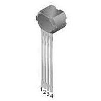
IC SWITCH BIPO DUAL OUT 4-SIP
Manufacturer
Allegro Microsystems Inc
Type
Bipolar Latchr
Datasheet
1.A3425LK-T.pdf
(21 pages)
Specifications of A3425EK-T
Sensing Range
35G Trip, -35G Release
Voltage - Supply
3.3 V ~ 18 V
Current - Supply
6mA
Current - Output (max)
20mA
Output Type
Digital, Open Drain
Features
Ultra Sensitive
Operating Temperature
-40°C ~ 85°C
Package / Case
4-SIP
Hall Effect Type
Bipolar
Output Current
70mA
Sensor Case Style
SIP
No. Of Pins
4
Supply Voltage Range
3.3V To 18V
Operating Temperature Range
-40°C To +85°C
Operating Temperature Max
85°C
Svhc
No SVHC (15-Dec-2010)
Rohs Compliant
Yes
Lead Free Status / RoHS Status
Lead free / RoHS Compliant


A3425
The device must be operated below the maximum junction
temperature of the device, T
peak conditions, reliable operation may require derating sup-
plied power or improving the heat dissipation properties of the
application. This section presents a procedure for correlating
factors affecting operating T
the Allegro MicroSystems Web site.)
The Package Thermal Resistance, R
marizing the ability of the application and the device to dissipate
heat from the junction (die), through all paths to the ambient air.
Its primary component is the Effective Thermal Conductivity,
K, of the printed circuit board, including adjacent devices and
traces. Radiation from the die through the device case, R
relatively small component of R
T
overmolding.
The effect of varying power levels (Power Dissipation, P
be estimated. The following formulas represent the fundamental
relationships used to estimate T
V
A worst-case estimate, P
able power level (V
at a selected R
For example, given common conditions such as: T
A
CC
, and air motion are signifi cant external factors, damped by
T = P
T = P
= 12 V, I
T
P
D
J
= T
= V
A
D
CC
+ T = 25°C + 7°C = 32°C
×
CC
JA
×
R
= 4 mA, and R
I
JA
and T
CC
P
T
CC(max)
D
J
= 12 V
= 48 mW
= T
= V
A
D(max)
.
A
D
IN
, I
+ ΔT
×
J(max)
J
CC(max)
×
×
. (Thermal data is also available on
, represents the maximum allow-
R
×
JA
4 mA = 48 mW
J
I
JA
JA
, at P
IN
. Under certain combinations of
140 °C/W = 7°C
. Ambient air temperature,
= 140 °C/W, then:
), without exceeding T
(2)
JA
D
.
, is a fi gure of merit sum-
Typical Thermal Performance
(1)
(3)
Ultra-Sensitive Dual-Channel Quadrature
A
= 25°C,
JC
D
), can
J(max)
, is
,
Example: Reliability for V
minimum-K PCB
Observe the worst-case ratings for the device, specifi cally:
R
I
Calculate the maximum allowable power level, P
invert equation 3:
This provides the allowable increase to T
power dissipation. Then, invert equation 2:
P
Finally, invert equation 1 with respect to voltage:
The result indicates that, at T
dissipate adequate amounts of heat at voltages ≤V
Compare V
able operation between V
R
V
CC(max)
JA
JA
CC(max)
V
T
D(max)
CC(est)
. If V
= 140 °C/W, T
max
= 6 mA.
is reliable under these conditions.
= T
= T
= P
CC(est)
Hall-Effect Bipolar Switch
CC(est)
J(max)
D(max)
max
≥ V
to V
J(max)
÷ R
– T
÷ I
CC(max)
JA
CC(max)
A
CC(max)
= 165°C, V
= 165 °C – 150 °C = 15 °C
= 15°C ÷ 140 °C/W = 107 mW
CC(est)
115 Northeast Cutoff, Box 15036
CC
Allegro MicroSystems, Inc.
Worcester, Massachusetts 01615-0036 (508) 853-5000
www.allegromicro.com
, then operation between V
A
. If V
at T
= 107 mW ÷ 6 mA = 18 V
, the application and device can
and V
A
CC(est)
= 150°C, package L, using
CC(max)
CC(max)
≤ V
J
resulting from internal
= 18 V, and
CC(max)
requires enhanced
D(max)
CC(est)
, then reli-
CC(est)
. First,
.
and
10
Related parts for A3425EK-T
Image
Part Number
Description
Manufacturer
Datasheet
Request
R

Part Number:
Description:
IC, HALL EFFECT SENSOR, Linear, SOIC-8
Manufacturer:
Allegro Microsystems Inc
Datasheet:
Part Number:
Description:
IC, HALL EFFECT SENSOR, Linear, SOIC-8
Manufacturer:
Allegro Microsystems Inc
Datasheet:
Part Number:
Description:
IC, HALL EFFECT SENSOR, Linear, SOIC-8
Manufacturer:
Allegro Microsystems Inc
Datasheet:

Part Number:
Description:
IC SWITCH INTERFACE 2CHAN 8-SOIC
Manufacturer:
Allegro Microsystems Inc
Datasheet:

Part Number:
Description:
IC SMOKE DETECTOR ION 16-DIP
Manufacturer:
Allegro Microsystems Inc
Datasheet:
Part Number:
Description:
IC SMOKE DETECTOR ION 16-DIP
Manufacturer:
Allegro Microsystems Inc
Datasheet:
Part Number:
Description:
IC SMOKE DETECTOR ION 16-DIP
Manufacturer:
Allegro Microsystems Inc
Datasheet:
Part Number:
Description:
IC SMOKE DETECTOR PHOTO 16-DIP
Manufacturer:
Allegro Microsystems Inc
Datasheet:
Part Number:
Description:
IC SMOKE DETECTOR ION 16-DIP
Manufacturer:
Allegro Microsystems Inc
Datasheet:
Part Number:
Description:
IC SMOKE DETECTOR PHOTO 16-DIP
Manufacturer:
Allegro Microsystems Inc
Datasheet:
Part Number:
Description:
IC SMOKE DETECTOR PHOTO 16-DIP
Manufacturer:
Allegro Microsystems Inc
Datasheet:
Part Number:
Description:
IC SMOKE DETECTOR ION 16-DIP
Manufacturer:
Allegro Microsystems Inc
Datasheet:
Part Number:
Description:
IC SMOKE DETECTOR PHOTO 16-SOIC
Manufacturer:
Allegro Microsystems Inc
Datasheet:

Part Number:
Description:
IC LED DRIVER HIGH BRIGHT 16-QFN
Manufacturer:
Allegro Microsystems Inc
Datasheet:

Part Number:
Description:
IC LED DRIVER AUTOMOTIVE 8-SOIC
Manufacturer:
Allegro Microsystems Inc
Datasheet: