HMC1021D Honeywell Microelectronics & Precision Sensors, HMC1021D Datasheet - Page 3
HMC1021D
Manufacturer Part Number
HMC1021D
Description
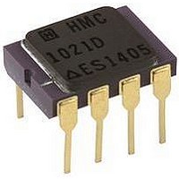
IC SENSOR MAGN HI TEMP CER 8DIP
Manufacturer
Honeywell Microelectronics & Precision Sensors
Type
Linearr
Series
-r
Specifications of HMC1021D
Sensing Range
±6g
Voltage - Supply
2 V ~ 25 V
Output Type
Differential Voltage
Features
Compass - One Axis
Operating Temperature
-55°C ~ 150°C
Package / Case
8-DIP
Supply Voltage Range
1.8V To 12V
Sensor Case Style
DIP
No. Of Pins
8
Hall Effect Type
Linear
Operating Temperature Range
-55°C To +225°C
Supply Voltage Min
1.8V
Operating Supply Voltage (typ)
5V
Current - Supply
-
Current - Output (max)
-
Lead Free Status / RoHS Status
Lead free / RoHS Compliant
Current - Supply
-
Current - Output (max)
-
Lead Free Status / Rohs Status
Not Compliant
Available stocks
Company
Part Number
Manufacturer
Quantity
Price
Company:

Part Number:
HMC1021D
Manufacturer:
SAGAMI
Quantity:
2 000


HMC1021D
PIN CONFIGURATION
(Arrow indicates direction of applied field that generates a positive output voltage after a SET pulse.)
BASIC DEVICE OPERATION
The Honeywell HMC1021D magneto-resistive sensor is composed of a Wheatstone bridge element to measure magnetic
fields for both field strength and direction. With power applied to the bridge, the sensor element converts any incident
magnetic field in the element’s sensitive axis direction to a differential voltage output. In addition to the bridge element, the
sensor has two types of on-chip magnetically coupled straps; the offset strap and the set/reset strap. These straps are
Honeywell patented features for incident field adjustment and magnetic domain alignment; and eliminate the need for
external coils positioned around the sensors.
The magnetoresistive sensor is made of a nickel-iron (Permalloy) thin-film deposited on a silicon wafer and patterned as a
resistive strip element die. Using semiconductor processes, the wafer is diced and packaged in a custom ceramic DIP IC
package with a low magnetic lead frame. In the presence of a magnetic field, a change in the bridge resistive element
causes a corresponding change in voltage across the bridge output (OUT – and OUT+ pins).
This resistive element is aligned to have a sensitive axis (indicated by the arrow on the pinout) that will provide positive
voltage change with magnetic fields increasing in the sensitive direction. Because the output only is in proportion to the
one-dimensional axis (the principle of anisotropy) and its magnitude, additional sensor bridges placed at orthogonal
directions permit accurate measurement of arbitrary field direction. The combination of sensor bridges in two or three
orthogonal axis configurations permit applications such as compassing and magnetometry.
The sensor offset strap allows for several modes of operation when a direct current is driven through it. These modes are:
1) Subtraction (bucking) of an unwanted external magnetic field, 2) null-ing of the bridge offset voltage, 3) Closed loop
field cancellation, and 4) Auto-calibration of bridge gain.
The set/reset strap can be pulsed with high currents for the following benefits: 1) Enable the sensor to perform high
sensitivity measurements, 2) Flip the polarity of the bridge output voltage, and 3) Periodically used to improve linearity,
lower cross-axis effects, and temperature effects.
Noise Characteristics
The noise density for the HMR1021D is around 50nV/sqrt Hz at the 1 Hz corner, and drops below 10nV/sqrt Hz at 20Hz
and begins to fit the Johnson Noise value at around 5nV/sqrt Hz beyond 100Hz. The 10Hz noise voltage averages around
0.58 micro-volts with a 0.16 micro-volts standard deviation. These values are provided with a 5-volt supply.
Offset Strap
The offset strap is a spiral of metallization that couples in the sensor element’s sensitive axis. The offset strap measures
nominally 50 ohms, and requires about 4.6mA for each gauss of induced field. The strap will easily handle currents to
buck or boost fields through the ±6 gauss linear measurement range, but designers should note the extreme thermal
heating on the sensor die when doing so.
With most applications, the offset strap is not utilized and can be ignored. Designers can leave one or both strap
connections (Off- and Off+) open circuited, or ground one connection node. Do not tie positive and negative strap
connections together of the same strap to avoid shorted turn magnetic circuits.
www.honeywell.com
VBRIDGE
VBRIDGE
OUT+ 1
OUT+ 1
GND
GND
OUT-
OUT-
2
2
3
3
4
4
DIE
DIE
DIE
DIE
8
8
7
7
6
6
5
5
OFFSET-
OFFSET-
OFFSET+
OFFSET+
S/R-
S/R-
S/R+
S/R+
3
Related parts for HMC1021D
Image
Part Number
Description
Manufacturer
Datasheet
Request
R

Part Number:
Description:
IC COMPASS 3 AXIS I2C 16LCC SMD
Manufacturer:
Honeywell Microelectronics & Precision Sensors
Datasheet:

Part Number:
Description:
SENSOR MAGNETIC 3 AXIS 20-LCC
Manufacturer:
Honeywell Microelectronics & Precision Sensors
Datasheet:

Part Number:
Description:
MAGNETIC SENSORS
Manufacturer:
Honeywell Microelectronics & Precision Sensors

Part Number:
Description:
MAGNETIC SENSORS
Manufacturer:
Honeywell Microelectronics & Precision Sensors
Part Number:
Description:
MAGNETIC SENSORS
Manufacturer:
Honeywell Microelectronics & Precision Sensors
Part Number:
Description:
MAGNETIC SENSORS
Manufacturer:
Honeywell Microelectronics & Precision Sensors
Part Number:
Description:
MAGNETIC SENSORS
Manufacturer:
Honeywell Microelectronics & Precision Sensors
Datasheet:
Part Number:
Description:
MAGNETIC SENSORS
Manufacturer:
Honeywell Microelectronics & Precision Sensors

Part Number:
Description:
MAGNETIC SENSORS
Manufacturer:
Honeywell Microelectronics & Precision Sensors
Datasheet:

Part Number:
Description:
MAGNETIC SENSORS
Manufacturer:
Honeywell Microelectronics & Precision Sensors
Datasheet:

Part Number:
Description:
SENSOR LINEAR MAGN 1 AXIS 8-SIP
Manufacturer:
Honeywell Microelectronics & Precision Sensors
Datasheet:

Part Number:
Description:
SENSOR MAGN 2 AXIS 10-MSOP
Manufacturer:
Honeywell Microelectronics & Precision Sensors
Datasheet:

Part Number:
Description:
Magnetic Sensor
Manufacturer:
Honeywell Microelectronics & Precision Sensors
Datasheet:

Part Number:
Description:
Magnetic Sensor
Manufacturer:
Honeywell Microelectronics & Precision Sensors
Datasheet:

Part Number:
Description:
IC, MAGNETO RESISTIVE SENSOR, LCC-16
Manufacturer:
Honeywell Microelectronics & Precision Sensors
Datasheet: