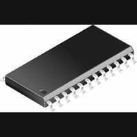
USBN9603-28M National Semiconductor, USBN9603-28M Datasheet - Page 53

USBN9603-28M
Manufacturer Part Number
USBN9603-28M
Description
USB Controller IC
Manufacturer
National Semiconductor
Specifications of USBN9603-28M
Interface
USB
No. Of Pins
28
Peak Reflow Compatible (260 C)
No
Supply Voltage Max
7V
Leaded Process Compatible
No
Controller Type, Ic
USB
Package / Case
28-WSOIC
Lead Free Status / RoHS Status
Contains lead / RoHS non-compliant
Available stocks
Company
Part Number
Manufacturer
Quantity
Price
Part Number:
USBN9603-28M
Manufacturer:
NS/国半
Quantity:
20 000
Company:
Part Number:
USBN9603-28M/NOPB
Manufacturer:
nsc
Quantity:
2 690
Company:
Part Number:
USBN9603-28MX
Manufacturer:
NSC
Quantity:
189
Part Number:
USBN9603-28MX
Manufacturer:
NS/国半
Quantity:
20 000
Company:
Part Number:
USBN9603-28MX/NOPB
Manufacturer:
NS
Quantity:
3 000
Part Number:
USBN9603-28MX/NOPB
Manufacturer:
NS/国半
Quantity:
20 000
8.0 Device Characteristics
8.3 AC ELECTRICAL CHARACTERISTICS
Oscillator Input/Output Signals (XTALIN, XTALOUT)
Voltage Regulator (3.3V)
Full Speed Signaling (D+, D-)
Clock Out Characteristics (CLKOUT)
(3.0V< V
Symbol
Symbol
T
C
1. If the internal voltage regulator is enabled, the minimum voltage is 4.25V instead of 3.0V.
2. CLKOUT is not driven and the device is not accessed.
3. The internal votlage regulator is disabled.
4. These voltage levels apply only when an external clock is connected to XTALIN.
5. Much lower voltage levels are expected when the internal oscillator is used.
6. Not tested. Guaranteed by design.
7. The internal voltage regulator is intended to power only the internal transceivers and one external pull-up.
T
V
Z
CYCLE
1. Testing is centered around 50 , not 45
2. Waveforms are measured from 10% to 90%.
C
V
XOUT
V
I
V
T
T
RFM
T
T
V
CRS
DRV
I
I
OZ
XIN
IH
IL
An external de-coupling capacitor is connected to this pin.
IH
R
F
R
F
IL
IL
O
CC
< 5.5V, 0˚C < TA< +70˚C, unless otherwise specified)
Rise Time
Fall Time
Rise / Fall Time Matching (T
Output Signal Crossover Voltage
Driver Output Impedance (Single Ended)
Output Rise Time
Output Fall Time
Output Duty Cycle
Input Low Voltage
Input Low Current
Input High Current
Tri-state Leakage
Input High Switching Level
Input Low Switching Level
Input Capacitance
Output Capacitance
Output Voltage
Parameter
Parameter
7
6
(Continued)
4, 5
4, 5
R
/T
V
V
V
F
)
IN
IN
OUT
+/-15% as specified in USB spec. rev 1.1.
= GND
= V
= V
CC
CC
53
Conditions
or GND
Conditions
Fout<48MHz
C
C
C
C
C
C
C
L
L
L
L
L
L
L
= 50pF
= 50pF
= 50pF
= 50pF
= 50pF
= 50pF
= 50pF
1 2
Min
-10
1.8
3.0
Min
1.3
90
45
4
4
Typ
Typ
35
Max
-10
0.8
1.0
4.0
4.0
3.6
10
10
Max
110
2.0
20
20
10
10
55
www.national.com
Units
Units
pF
pF
V
V
V
V
nS
nS
nS
nS
%
%
V
A
A
A


