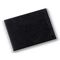
S29JL032H70TFI010 Spansion Inc., S29JL032H70TFI010 Datasheet - Page 39

S29JL032H70TFI010
Manufacturer Part Number
S29JL032H70TFI010
Description
IC, FLASH, 32MBIT, 70NS, TSOP-48
Manufacturer
Spansion Inc.
Datasheet
1.S29JL032H90TFI320.pdf
(61 pages)
Specifications of S29JL032H70TFI010
Memory Type
Flash
Memory Size
32Mbit
Memory Configuration
4M X 8 / 2M X 16
Ic Interface Type
Parallel
Access Time
70ns
Supply Voltage Range
2.7V To 3.6V
Memory Case Style
TSOP
No. Of Pins
48
Lead Free Status / RoHS Status
Lead free / RoHS Compliant
Available stocks
Company
Part Number
Manufacturer
Quantity
Price
Company:
Part Number:
S29JL032H70TFI010D
Manufacturer:
MIT
Quantity:
649
Company:
Part Number:
S29JL032H70TFI010H
Manufacturer:
ANACHIP
Quantity:
1 950
11.2
11.3
August 31, 2009 S29JL032H_00_B8
RY/BY#: Ready/Busy#
DQ6: Toggle Bit I
Notes
1. VA = Valid address for programming. During a sector erase operation, a valid address is any sector address within the sector being
2. DQ7 should be rechecked even if DQ5 = “1” because DQ7 may change simultaneously with DQ5.
The RY/BY# is a dedicated, open-drain output pin which indicates whether an Embedded Algorithm is in
progress or complete. The RY/BY# status is valid after the rising edge of the final WE# pulse in the command
sequence. Since RY/BY# is an open-drain output, several RY/BY# pins can be tied together in parallel with a
pull-up resistor to V
If the output is low (Busy), the device is actively erasing or programming. (This includes programming in the
Erase Suspend mode.) If the output is high (Ready), the device is in the read mode, the standby mode, or one
of the banks is in the erase-suspend-read mode.
Table 11.1 on page 42
Toggle Bit I on DQ6 indicates whether an Embedded Program or Erase algorithm is in progress or complete,
or whether the device has entered the Erase Suspend mode. Toggle Bit I may be read at any address, and is
valid after the rising edge of the final WE# pulse in the command sequence (prior to the program or erase
operation), and during the sector erase time-out.
During an Embedded Program or Erase algorithm operation, successive read cycles to any address cause
DQ6 to toggle. The system may use either OE# or CE# to control the read cycles. When the operation is
complete, DQ6 stops toggling.
erased. During chip erase, a valid address is any non-protected sector address.
CC
.
shows the outputs for RY/BY#.
D a t a
No
S h e e t
Figure 11.1 Data# Polling Algorithm
S29JL032H
Read DQ7–DQ0
Read DQ7–DQ0
DQ7 = Data?
DQ7 = Data?
Addr = VA
Addr = VA
DQ5 = 1?
START
FAIL
No
Yes
No
Yes
Yes
PASS
39


