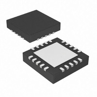
PIC16HV785-E/ML Microchip Technology, PIC16HV785-E/ML Datasheet - Page 25

PIC16HV785-E/ML
Manufacturer Part Number
PIC16HV785-E/ML
Description
3.5KB Flash, 128 RAM, 18 I/O 20 QFN 4x4mm TUBE
Manufacturer
Microchip Technology
Series
PIC® 16Fr
Datasheets
1.PIC16F616T-ISL.pdf
(8 pages)
2.PIC16F785-ISS.pdf
(206 pages)
3.PIC16F785-ISS.pdf
(10 pages)
4.PIC16F785-ISS.pdf
(28 pages)
Specifications of PIC16HV785-E/ML
Core Processor
PIC
Core Size
8-Bit
Speed
20MHz
Peripherals
Brown-out Detect/Reset, POR, PWM, WDT
Number Of I /o
17
Program Memory Size
3.5KB (2K x 14)
Program Memory Type
FLASH
Eeprom Size
256 x 8
Ram Size
128 x 8
Voltage - Supply (vcc/vdd)
2 V ~ 5.5 V
Data Converters
A/D 14x10b
Oscillator Type
Internal
Operating Temperature
-40°C ~ 125°C
Package / Case
20-VQFN Exposed Pad, 20-HVQFN, 20-SQFN, 20-DHVQFN
Processor Series
PIC16H
Core
PIC
Data Bus Width
8 bit
Data Ram Size
128 B
Interface Type
RS- 232, USB
Maximum Clock Frequency
32 MHz
Number Of Programmable I/os
18
Number Of Timers
3
Maximum Operating Temperature
+ 125 C
Mounting Style
SMD/SMT
3rd Party Development Tools
52715-96, 52716-328, 52717-734
Development Tools By Supplier
PG164130, DV164035, DV244005, DV164005, PG164120, ICE2000, DV164120, DM163029
Minimum Operating Temperature
- 40 C
On-chip Adc
10 bit, 14 Channel
Lead Free Status / RoHS Status
Lead free / RoHS Compliant
For Use With
AC164324 - MODULE SKT FOR MPLAB 8DFN/16QFN
Connectivity
-
Lead Free Status / Rohs Status
Details
Available stocks
Company
Part Number
Manufacturer
Quantity
Price
Company:
Part Number:
PIC16HV785-E/ML
Manufacturer:
LEGERITY
Quantity:
100
TABLE 5-1:
5.3.2
The programmer should be able to read data memory
information from a hex file and conversely (as an
option), write data memory contents to a hex file along
with program memory information and Configuration
Word
information.
The 256 data memory locations are logically mapped
starting at address 0x2100. The format for data
memory storage is one data byte per address location,
LSb aligned.
2009 Microchip Technology Inc.
PIC16F785/HV785
Legend: CFGW = Configuration Word. Example calculations assume Configuration Word is erased (all 1’s).
Note 1:
Device
(0x2007)
SUM[a:b] = [Sum of locations a to b inclusive]
SUM_ID = User ID locations masked by 0xF then made into a 16-bit value with ID0 as the Most Significant
nibble.
* = Checksum
+ = Addition
& = Bitwise AND
Checksum shown assumes that both the data and program memory are code-protected and that SUM_ID
contains the unprotected checksum.
EMBEDDING DATA MEMORY
CONTENTS IN HEX FILE
For example, ID0 = 0x1, ID1 = 0x2, ID3 = 0x3, ID4 = 0x4, then SUM_ID = 0x1234.
The 4 LSbs of the unprotected checksum is used for the example calculations.
CHECKSUM COMPUTATIONS
and
Code-Protect
user
– [
Sum of all the individual expressions] MODULO [0xFFFF]
OFF
ALL
ID
(0x2000-0x2003)
SUM[0x0000:0x7FF] + CFGW & 0FFF
CFGW & 0x0FFF + SUM_ID
Checksum*
PIC16F785/HV785
173E
Blank
Value
07FF
(1)
DS41237D-page 25
0x25E6 at 0
and Max.
Address
E30C
D3CD
(1)


