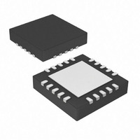
PIC16HV785-E/ML Microchip Technology, PIC16HV785-E/ML Datasheet - Page 143

PIC16HV785-E/ML
Manufacturer Part Number
PIC16HV785-E/ML
Description
3.5KB Flash, 128 RAM, 18 I/O 20 QFN 4x4mm TUBE
Manufacturer
Microchip Technology
Series
PIC® 16Fr
Datasheets
1.PIC16F616T-ISL.pdf
(8 pages)
2.PIC16F785-ISS.pdf
(206 pages)
3.PIC16F785-ISS.pdf
(10 pages)
4.PIC16F785-ISS.pdf
(28 pages)
Specifications of PIC16HV785-E/ML
Core Processor
PIC
Core Size
8-Bit
Speed
20MHz
Peripherals
Brown-out Detect/Reset, POR, PWM, WDT
Number Of I /o
17
Program Memory Size
3.5KB (2K x 14)
Program Memory Type
FLASH
Eeprom Size
256 x 8
Ram Size
128 x 8
Voltage - Supply (vcc/vdd)
2 V ~ 5.5 V
Data Converters
A/D 14x10b
Oscillator Type
Internal
Operating Temperature
-40°C ~ 125°C
Package / Case
20-VQFN Exposed Pad, 20-HVQFN, 20-SQFN, 20-DHVQFN
Processor Series
PIC16H
Core
PIC
Data Bus Width
8 bit
Data Ram Size
128 B
Interface Type
RS- 232, USB
Maximum Clock Frequency
32 MHz
Number Of Programmable I/os
18
Number Of Timers
3
Maximum Operating Temperature
+ 125 C
Mounting Style
SMD/SMT
3rd Party Development Tools
52715-96, 52716-328, 52717-734
Development Tools By Supplier
PG164130, DV164035, DV244005, DV164005, PG164120, ICE2000, DV164120, DM163029
Minimum Operating Temperature
- 40 C
On-chip Adc
10 bit, 14 Channel
Lead Free Status / RoHS Status
Lead free / RoHS Compliant
For Use With
AC164324 - MODULE SKT FOR MPLAB 8DFN/16QFN
Connectivity
-
Lead Free Status / Rohs Status
Details
Available stocks
Company
Part Number
Manufacturer
Quantity
Price
Company:
Part Number:
PIC16HV785-E/ML
Manufacturer:
LEGERITY
Quantity:
100
19.0
Absolute Maximum Ratings
Ambient temperature under bias................................................................................................................. -40 to +125°C
Storage temperature .............................................................................................................................. -65°C to +150°C
Voltage on V
Voltage on MCLR with respect to Vss ........................................................................................................-0.3 to +13.5V
Voltage on RB6 open-drain pin with respect to Vss .....................................................................................-0.3 to +8.5V
Voltage on all other pins with respect to V
Total power dissipation
Total power dissipation
Maximum current out of V
Maximum current into V
Input clamp current, I
Output clamp current, I
Maximum output current sunk by any I/O pin..........................................................................................................25 mA
Maximum output current sourced by any I/O pin ....................................................................................................25 mA
Maximum current sunk by PORTA, PORTB, and PORTC (combined) .................................................................200 mA
Maximum current sourced PORTA, PORTB, and PORTC (combined).................................................................200 mA
Note 1:
© 2008 Microchip Technology Inc.
† NOTICE: Stresses above those listed under “Absolute Maximum Ratings” may cause permanent damage to the
device. This is a stress rating only and functional operation of the device at those or any other conditions above those
indicated in the operation listings of this specification is not implied. Exposure to maximum rating conditions for
extended periods may affect device reliability.
Note:
ELECTRICAL SPECIFICATIONS
Power dissipation is calculated as follows: P
Voltage spikes below V
Thus, a series resistor of 50-100
pulling this pin directly to V
DD
with respect to V
IK
(1)
(1)
OK
(V
DD
(PDIP and SOIC).........................................................................................................800 mW
(SSOP) ........................................................................................................................600 mW
I
SS
(Vo < 0 or Vo >V
< 0 or V
pin ..............................................................................................................................250 mA
pin ...........................................................................................................................300 mA
(†)
SS
I
SS
> V
............................................................................................................ -0.3 to +6.5V
SS
at the MCLR pin, inducing currents greater than 80 mA, may cause latch-up.
DD
.
SS
)...................................................................................................................... ±20 mA
DD
Ω
................................................................................. -0.3V to (V
)................................................................................................................ ±20 mA
should be used when applying a “low” level to the MCLR pin, rather than
DIS
= V
DD
x {I
DD
– ∑ I
PIC16F785/HV785
OH
} + ∑ {(V
DD
– V
OH
) x I
DS41249E-page 141
OH
} + ∑(V
DD
O
+ 0.3V)
l x I
OL
).


