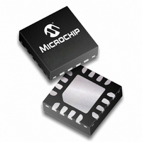
PIC16F676T-I/ML Microchip Technology, PIC16F676T-I/ML Datasheet - Page 9

PIC16F676T-I/ML
Manufacturer Part Number
PIC16F676T-I/ML
Description
1.75KB Flash, 64 RAM, 12 I/O 16 QFN 4x4mm T/R
Manufacturer
Microchip Technology
Series
PIC® 16Fr
Datasheets
1.PIC16F616T-ISL.pdf
(8 pages)
2.PIC12F629T-ISN.pdf
(24 pages)
3.PIC16F630-ISL.pdf
(132 pages)
4.PIC16F630-ISL.pdf
(2 pages)
5.PIC16F630-ISL.pdf
(10 pages)
Specifications of PIC16F676T-I/ML
Core Processor
PIC
Core Size
8-Bit
Speed
20MHz
Peripherals
Brown-out Detect/Reset, POR, WDT
Number Of I /o
12
Program Memory Size
1.75KB (1K x 14)
Program Memory Type
FLASH
Eeprom Size
128 x 8
Ram Size
64 x 8
Voltage - Supply (vcc/vdd)
2 V ~ 5.5 V
Data Converters
A/D 8x10b
Oscillator Type
Internal
Operating Temperature
-40°C ~ 85°C
Package / Case
16-QFN
Lead Free Status / RoHS Status
Lead free / RoHS Compliant
For Use With
AC164324 - MODULE SKT FOR MPLAB 8DFN/16QFN
Connectivity
-
Lead Free Status / RoHS Status
Lead free / RoHS Compliant, Lead free / RoHS Compliant
Available stocks
Company
Part Number
Manufacturer
Quantity
Price
Company:
Part Number:
PIC16F676T-I/ML
Manufacturer:
SHARP
Quantity:
124
2.0
2.1
The PIC16F630/676 devices have a 13-bit program
counter capable of addressing an 8K x 14 program
memory space. Only the first 1K x 14 (0000h-03FFh)
for the PIC16F630/676 devices is physically imple-
mented. Accessing a location above these boundaries
will cause a wrap around within the first 1K x 14 space.
The Reset vector is at 0000h and the interrupt vector is
at 0004h (see Figure 2-1).
FIGURE 2-1:
2010 Microchip Technology Inc.
CALL, RETURN
RETFIE, RETLW
MEMORY ORGANIZATION
Program Memory Organization
On-chip Program
Interrupt Vector
Stack Level 1
Stack Level 2
Stack Level 8
Reset Vector
PC<12:0>
Memory
PROGRAM MEMORY MAP
AND STACK FOR THE
PIC16F630/676
13
000h
0004
0005
03FFh
0400h
1FFFh
2.2
The data memory (see Figure 2-2) is partitioned into
two banks, which contain the General Purpose Regis-
ters and the Special Function Registers. The Special
Function Registers are located in the first 32 locations
of each bank. Register locations 20h-5Fh are General
Purpose Registers, implemented as static RAM and
are mapped across both banks. All other RAM is
unimplemented and returns ‘0’ when read. RP0
(STATUS<5>) is the bank select bit.
• RP0 = 0 Bank 0 is selected
• RP0 = 1 Bank 1 is selected
2.2.1
The register file is organized as 64 x 8 in the
PIC16F630/676 devices. Each register is accessed,
either directly or indirectly, through the File Select
Register FSR (see Section 2.4 “Indirect Addressing,
INDF and FSR Registers”).
Note:
Data Memory Organization
The IRP and RP1 bits STATUS<7:6> are
reserved and should always be maintained
as ‘0’s.
GENERAL PURPOSE REGISTER
FILE
PIC16F630/676
DS40039F-page 9


