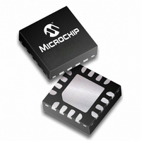
PIC16F610-E/ML Microchip Technology, PIC16F610-E/ML Datasheet - Page 78

PIC16F610-E/ML
Manufacturer Part Number
PIC16F610-E/ML
Description
1.75KB Flash, 64B RAM, 6 I/O, 8MHz Internal Oscillator 16 QFN 4x4mm TUBE
Manufacturer
Microchip Technology
Series
PIC® 16Fr
Datasheets
1.PIC12F609T-ISN.pdf
(26 pages)
2.PIC16F616T-ISL.pdf
(214 pages)
3.PIC16F616T-ISL.pdf
(8 pages)
Specifications of PIC16F610-E/ML
Core Processor
PIC
Core Size
8-Bit
Speed
20MHz
Peripherals
Brown-out Detect/Reset, POR, PWM, WDT
Number Of I /o
11
Program Memory Size
1.75KB (1K x 14)
Program Memory Type
FLASH
Ram Size
64 x 8
Voltage - Supply (vcc/vdd)
2 V ~ 5.5 V
Oscillator Type
Internal
Operating Temperature
-40°C ~ 125°C
Package / Case
16-QFN
Lead Free Status / RoHS Status
Lead free / RoHS Compliant
For Use With
AC162083 - HEADER MPLAB ICD2 PIC16F616 8/14AC164324 - MODULE SKT FOR MPLAB 8DFN/16QFNXLT16QFN1 - SOCKET TRANSITION 14DIP TO 16QFN
Eeprom Size
-
Data Converters
-
Connectivity
-
Lead Free Status / RoHS Status
Lead free / RoHS Compliant, Lead free / RoHS Compliant
- Current page: 78 of 214
- Download datasheet (4Mb)
PIC16F610/616/16HV610/616
9.2.7
The following registers are used to control the operation of the ADC.
REGISTER 9-1:
DS41288F-page 78
bit 7
Legend:
R = Readable bit
-n = Value at POR
bit 7
bit 6
bit 5-2
bit 1
bit 0
Note 1:
ADFM
R/W-0
When the CHS<3:0> bits change to select the 1.2V or 0.6V Fixed Voltage Reference, the reference output voltage will
have a transient. If the Comparator module uses this VP6 reference voltage, the comparator output may momentarily
change state due to the transient.
ADC REGISTER DEFINITIONS
ADFM: A/D Conversion Result Format Select bit
1 = Right justified
0 = Left justified
VCFG: Voltage Reference bit
1 = V
0 = V
CHS<3:0>: Analog Channel Select bits
0000 = Channel 00 (AN0)
0001 = Channel 01 (AN1)
0010 = Channel 02 (AN2)
0011 = Channel 03 (AN3)
0100 = Channel 04 (AN4)
0101 = Channel 05 (AN5)
0110 = Channel 06 (AN6)
0111 = Channel 07 (AN7)
1000 = Reserved – do not use
1001 = Reserved – do not use
1010 = Reserved – do not use
1011 = Reserved – do not use
1100 = CV
1101 = 0.6V Fixed Voltage Reference
1110 = 1.2V Fixed Voltage Reference
1111 = Reserved – do not use
GO/DONE: A/D Conversion Status bit
1 = A/D conversion cycle in progress. Setting this bit starts an A/D conversion cycle.
0 = A/D conversion completed/not in progress
ADON: ADC Enable bit
1 = ADC is enabled
0 = ADC is disabled and consumes no operating current
VCFG
This bit is automatically cleared by hardware when the A/D conversion has completed.
R/W-0
REF
DD
ADCON0: A/D CONTROL REGISTER 0
pin
REF
W = Writable bit
‘1’ = Bit is set
CHS3
R/W-0
CHS2
R/W-0
(1)
(1)
U = Unimplemented bit, read as ‘0’
‘0’ = Bit is cleared
CHS1
R/W-0
CHS0
R/W-0
© 2009 Microchip Technology Inc.
x = Bit is unknown
GO/DONE
R/W-0
ADON
R/W-0
bit 0
Related parts for PIC16F610-E/ML
Image
Part Number
Description
Manufacturer
Datasheet
Request
R

Part Number:
Description:
IC PIC MCU FLASH 1KX14 14DIP
Manufacturer:
Microchip Technology
Datasheet:

Part Number:
Description:
IC PIC MCU FLASH 1KX14 16QFN
Manufacturer:
Microchip Technology
Datasheet:

Part Number:
Description:
IC PIC MCU FLASH 1KX14 14SOIC
Manufacturer:
Microchip Technology
Datasheet:

Part Number:
Description:
IC PIC MCU FLASH 1KX14 14TSSOP
Manufacturer:
Microchip Technology
Datasheet:

Part Number:
Description:
1.75KB Flash, 64B RAM, 6 I/O, 8MHz Internal Oscillator 14 PDIP .300in TUBE
Manufacturer:
Microchip Technology
Datasheet:

Part Number:
Description:
1.75KB Flash, 64B RAM, 6 I/O, 8MHz Internal Oscillator 14 SOIC .150in TUBE
Manufacturer:
Microchip Technology
Datasheet:

Part Number:
Description:
1.75KB Flash, 64B RAM, 6 I/O, 8MHz Internal Oscillator 14 TSSOP 4.4mm TUBE
Manufacturer:
Microchip Technology
Datasheet:

Part Number:
Description:
IC, 8BIT MCU, PIC16F, 32MHZ, SOIC-18
Manufacturer:
Microchip Technology
Datasheet:

Part Number:
Description:
IC, 8BIT MCU, PIC16F, 32MHZ, SSOP-20
Manufacturer:
Microchip Technology
Datasheet:

Part Number:
Description:
IC, 8BIT MCU, PIC16F, 32MHZ, DIP-18
Manufacturer:
Microchip Technology
Datasheet:

Part Number:
Description:
IC, 8BIT MCU, PIC16F, 32MHZ, QFN-28
Manufacturer:
Microchip Technology
Datasheet:

Part Number:
Description:
IC, 8BIT MCU, PIC16F, 32MHZ, QFN-28
Manufacturer:
Microchip Technology
Datasheet:

Part Number:
Description:
IC, 8BIT MCU, PIC16F, 32MHZ, QFN-28
Manufacturer:
Microchip Technology
Datasheet:

Part Number:
Description:
IC, 8BIT MCU, PIC16F, 32MHZ, SSOP-20
Manufacturer:
Microchip Technology
Datasheet:

Part Number:
Description:
IC, 8BIT MCU, PIC16F, 20MHZ, DIP-40
Manufacturer:
Microchip Technology
Datasheet:


