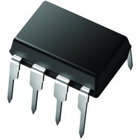
PIC12CE674-04E/P Microchip Technology, PIC12CE674-04E/P Datasheet - Page 424

PIC12CE674-04E/P
Manufacturer Part Number
PIC12CE674-04E/P
Description
IC,MICROCONTROLLER,8-BIT,PIC CPU,CMOS,DIP,8PIN,PLASTIC
Manufacturer
Microchip Technology
Series
PIC® 12Cr
Datasheets
1.PIC16F688T-ISL.pdf
(688 pages)
2.PIC12CE673-10P.pdf
(129 pages)
3.PIC12CE673-10P.pdf
(3 pages)
4.PIC12CE673-10P.pdf
(14 pages)
5.PIC12CE673-10P.pdf
(12 pages)
Specifications of PIC12CE674-04E/P
Rohs Compliant
YES
Core Processor
PIC
Core Size
8-Bit
Speed
4MHz
Peripherals
POR, WDT
Number Of I /o
5
Program Memory Size
3.5KB (2K x 14)
Program Memory Type
OTP
Eeprom Size
16 x 8
Ram Size
128 x 8
Voltage - Supply (vcc/vdd)
3 V ~ 5.5 V
Data Converters
A/D 4x8b
Oscillator Type
Internal
Operating Temperature
-40°C ~ 125°C
Package / Case
8-DIP (0.300", 7.62mm)
Processor Series
PIC12C
Core
PIC
Data Bus Width
8 bit
Data Ram Size
128 B
Maximum Clock Frequency
4 MHz
Number Of Programmable I/os
5
Number Of Timers
8
Maximum Operating Temperature
+ 125 C
Mounting Style
Through Hole
3rd Party Development Tools
52715-96, 52716-328, 52717-734
Development Tools By Supplier
ICE2000
Minimum Operating Temperature
- 40 C
On-chip Adc
8 bit
Lead Free Status / RoHS Status
Lead free / RoHS Compliant
Connectivity
-
Lead Free Status / Rohs Status
Details
Available stocks
Company
Part Number
Manufacturer
Quantity
Price
Company:
Part Number:
PIC12CE674-04E/P
Manufacturer:
MICROCHIP
Quantity:
12 000
- PIC16F688T-ISL PDF datasheet
- PIC12CE673-10P PDF datasheet #2
- PIC12CE673-10P PDF datasheet #3
- PIC12CE673-10P PDF datasheet #4
- PIC12CE673-10P PDF datasheet #5
- Current page: 424 of 688
- Download datasheet (3Mb)
PICmicro MID-RANGE MCU FAMILY
23.1
Figure 23-1:
DS31023A-page 23-2
Converter
10-bit
Introduction
A/D
10-bit A/D Block Diagram
Reference
voltage
The analog-to-digital (A/D) converter module can have up to eight analog inputs for a device.
The analog input charges a sample and hold capacitor. The output of the sample and hold capac-
itor is the input into the converter. The converter then generates a digital result of this analog level
via successive approximation. This A/D conversion, of the analog input signal, results in a corre-
sponding 10-bit digital number.
The analog reference voltages (positive and negative supply) are software selectable to either
the device’s supply voltages (AV
pins.
The A/D converter has a unique feature of being able to operate while the device is in SLEEP
mode.
The A/D module has four registers. These registers are:
The ADCON0 register, shown in
ADCON1 register, shown in
can be configured as analog inputs (AN3 and AN2 can also be the voltage references) or as dig-
ital I/O.
• A/D Result High Register (ADRESH)
• A/D Result Low Register (ADRESL)
• A/D Control Register0 (ADCON0)
• A/D Control Register1 (ADCON1)
V
V
REF
REF
-
+
(Input voltage)
V
AIN
PCFG0
Preliminary
Figure
DD
AV
Figure
, AVss) or the voltage level on the AN3/V
23-2, configures the functions of the port pins. The port pins
DD
AV
23-1, controls the operation of the A/D module. The
SS
CHS2:CHS0
111
110
101
100
011
010
001
000
1997 Microchip Technology Inc.
REF
AN1
AN7
AN6
AN5
AN4
AN3
AN2
AN0
+ and AN2/V
REF
-
Related parts for PIC12CE674-04E/P
Image
Part Number
Description
Manufacturer
Datasheet
Request
R

Part Number:
Description:
IC MCU OTP 2KX14 A/D&EE 8DIP
Manufacturer:
Microchip Technology
Datasheet:

Part Number:
Description:
IC MCU OTP 2KX14 A/D&EE 8DIP
Manufacturer:
Microchip Technology
Datasheet:

Part Number:
Description:
IC MCU OTP 2KX14 A/D&EE 8DIP
Manufacturer:
Microchip Technology
Datasheet:

Part Number:
Description:
IC MCU EPROM 2KX14 A/D&EE 8CDIP
Manufacturer:
Microchip Technology
Datasheet:

Part Number:
Description:
IC MCU OTP 2KX14 A/D&EE 8DIP
Manufacturer:
Microchip Technology
Datasheet:

Part Number:
Description:
IC MCU OTP 2KX14 A/D&EE 8DIP
Manufacturer:
Microchip Technology
Datasheet:

Part Number:
Description:
8-Pin/ 8-Bit CMOS Microcontroller with A/D Converter and EEPROM Data Memory
Manufacturer:
Microchip Technology
Datasheet:

Part Number:
Description:
Manufacturer:
Microchip Technology Inc.
Datasheet:

Part Number:
Description:
Manufacturer:
Microchip Technology Inc.
Datasheet:

Part Number:
Description:
Manufacturer:
Microchip Technology Inc.
Datasheet:

Part Number:
Description:
Manufacturer:
Microchip Technology Inc.
Datasheet:

Part Number:
Description:
Manufacturer:
Microchip Technology Inc.
Datasheet:


