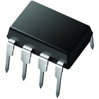
PIC10F220-E/P Microchip Technology, PIC10F220-E/P Datasheet

PIC10F220-E/P
Specifications of PIC10F220-E/P
Related parts for PIC10F220-E/P
PIC10F220-E/P Summary of contents
Page 1
... PIC10F222 1.0 PROGRAMMING THE PIC10F220/222 The PIC10F220/222 is programmed using a serial method. The Serial mode will allow the PIC10F220/222 to be programmed while in the user’s system. This allows for increased design flexibility. This programming specification applies to PIC10F220/222 devices in all packages. Pin Diagrams ...
Page 2
... In the configuration memory space, 0x100-0x13F for the PIC10F220 and 0x200-0x23F for the PIC10F222 are physically implemented. However, only locations 0x100-0x103 and 0x200-0x203 are available. Other locations are reserved. ...
Page 3
... The programming sequence loads a word, programs, verifies and finally increments the PC. Program/Verify mode entry will set the address to 0x1FF for the PIC10F220 and 0x3FF for the PIC10F222. The Increment Address command will increment the PC. The available commands are shown in Table 3-1. ...
Page 4
... PIC10F220/222 TABLE 3-1: COMMAND MAPPING FOR PIC10F220/222 Command Load Data for Program Memory Read Data from Program Memory Increment Address Begin Programming End Programming Bulk Erase Program Memory 3.1.2.1 Load Data For Program Memory After receiving this command, the chip will load in a 14-bit “ ...
Page 5
... A timing diagram of this command is shown in Figure 3- not possible to decrement the address counter. To reset this counter, the user must either exit and re-enter Program/Verify mode or increment the PC from 0x1FF for the PIC10F220 or 0x3FF for the PIC10F222 to 0x000. FIGURE 3-5: INCREMENT ADDRESS COMMAND 1 ...
Page 6
... PIC10F220/222 3.1.2.5 End Programming The End Programming command terminates the program process. A delay of T (see Table 6-1) is DIS required before the next command to allow the internal programming voltage to discharge (see Figure 3-7). FIGURE 3-7: END PROGRAMMING (EXTERNALLY TIMED) 1 ICSPCLK 0 ICSPDAT 3.1.2.6 ...
Page 7
... Configuration Word or Program Memory Space First User ID Location FIGURE 3-8: BULK ERASE PROGRAM MEMORY COMMAND 1 2 ICSPCLK 1 ICSPDAT T 1 SET T HLD © 2007 Microchip Technology Inc. Configuration Reset Vector Word PIC10F220/222 Configuration Memory Space Backup User ID OSCCAL ERA Next Command 1 2 DS41266C-page 7 ...
Page 8
... PIC10F220/222 FIGURE 3-9: READING AND TEMPORARY SAVING OF THE OSCCAL CALIBRATION BITS Increment Address Increment Address DS41266C-page 8 Start Enter Programming Mode 0x0FF/0x1FF? Yes Read Calibration Bits and Save in Computer/Programmer Temp. Memory 0x104/0x204? Yes Read Backup OSCCAL Calibration Bits and Save in Computer/Programmer Temp. Memory ...
Page 9
... FIGURE 3-10: RESTORING/PROGRAMMING THE OSCCAL CALIBRATION BITS Increment Address Increment Address © 2007 Microchip Technology Inc. PIC10F220/222 Start Enter Programming Mode 0x0FF/0x1FF? Yes Read Calibration Bits from Computer/Programmer Temp. Memory Write Calibration Bits back as the operand of a MOVLW instruction to 0x0FF/0x1FF 0x104/0x204? ...
Page 10
... PIC10F220/222 FIGURE 3-11: PROGRAM FLOWCHART – PIC10F220/222 PROGRAM MEMORY Start Read and save OSCCAL bits ( Figure 3-9 Enter Programing Mode PC = 0x1FF/0x3FF (Config Word) Increment Address Bulk Erase Device One-Word Program Cycle Read Data from Program Memory Data Correct? Yes Increment No Address ...
Page 11
... FIGURE 3-12: PROGRAM FLOWCHART – PIC10F220/222 CONFIGURATION MEMORY Start Enter Programming Mode PC = 0x1FF/0x3FF (Config Word) Load Data Command One-Word Programming Cycle (see Figure 3-11) Read Data Command Data Correct? Yes Increment Address Command No Address = 0x100/0x200 Yes Load Data Command One-Word Programming ...
Page 12
... PIC10F220/222 FIGURE 3-13: PROGRAM FLOWCHART – ERASE PROGRAM MEMORY, CONFIGURATION WORD Start Read and save OSCCAL bits Figure 3 Enter Program/Verify mode PC = 0x1FF/0x3FF (Config Word) FIGURE 3-14: PROGRAM FLOWCHART – ERASE PROGRAM MEMORY, CONFIGURATION WORD AND USER ID Start Increment PC DS41266C-page 12 Bulk Erase Device ...
Page 13
... CONFIGURATION WORD The PIC10F220/222 has several Configuration bits. These bits can be programmed (reads ‘0’) or left unchanged (reads ‘1’), to select various device configurations. REGISTER 4-1: CONFIGURATION WORD PIC10F220/222 — — — — bit 11 bit 11-5 Unimplemented: Read as ‘1’ ...
Page 14
... Checksum Computation 5.3.1 CHECKSUM Checksum is calculated by reading the contents of the PIC10F220/222 memory locations and adding up the opcodes up to the maximum user addressable location (e.g., 0x1FF for the PIC10F222). Any Carry bits exceeding 16 bits are neglected. Finally, the Configuration Word (appropriately masked) is added to the checksum ...
Page 15
... TABLE 5-1: CHECKSUM COMPUTATIONS – PIC10F220 Device Code-Protect PIC10F220 OFF SUM[0x000:0x0FE] + CFGW & 0x01F ON SUM[0x00:0x3F] + CFGW & 0x01F + SUM_ID Legend: CFGW = Configuration Word SUM[a:b] = [Sum of locations inclusive] SUM_ID = User ID locations masked by 0xF then made into a 16-bit value with ID0 as the Most Significant nibble ...
Page 16
... PIC10F220/222 6.0 PROGRAM/VERIFY MODE ELECTRICAL CHARACTERISTICS TABLE 6-1: AC/DC CHARACTERISTICS TIMING REQUIREMENTS FOR PROGRAM/VERIFY MODE AC/DC CHARACTERISTICS Sym. Characteristics General V V level for programming operations, DDPROG DD program memory V V level for Bulk Erase operations, DDERA DD program memory I I level for programming operations, ...
Page 17
... PowerInfo, PowerMate, PowerTool, REAL ICE, rfLAB, Select Mode, Smart Serial, SmartTel, Total Endurance, UNI/O, WiperLock and ZENA are trademarks of Microchip Technology Incorporated in the U.S.A. and other countries. SQTP is a service mark of Microchip Technology Incorporated in the U.S.A. All other trademarks mentioned herein are property of their respective companies. ...
Page 18
... Fax: 886-3-572-6459 Taiwan - Kaohsiung Tel: 886-7-536-4818 Fax: 886-7-536-4803 Taiwan - Taipei Tel: 886-2-2500-6610 Fax: 886-2-2508-0102 Thailand - Bangkok Tel: 66-2-694-1351 Fax: 66-2-694-1350 © 2007 Microchip Technology Inc. EUROPE Austria - Wels Tel: 43-7242-2244-39 Fax: 43-7242-2244-393 Denmark - Copenhagen Tel: 45-4450-2828 Fax: 45-4485-2829 France - Paris Tel: 33-1-69-53-63-20 ...


