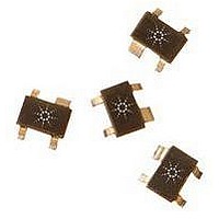
MGA-71543-BLK Avago Technologies US Inc., MGA-71543-BLK Datasheet - Page 18

MGA-71543-BLK
Manufacturer Part Number
MGA-71543-BLK
Description
Amplifier IC
Manufacturer
Avago Technologies US Inc.
Datasheet
1.MGA-71543-BLK.pdf
(24 pages)
Specifications of MGA-71543-BLK
No. Of Amplifiers
1
No. Of Pins
4
Noise Figure Typ
0.8dB
Gain
16dB
Power @ 1db Gain Compression, P1db
15.5
Mounting Type
Surface Mount
Packaging Type
Cut Tape
Peak Reflow Compatible (260 C)
No
Lead Free Status / RoHS Status
Contains lead / RoHS non-compliant
Available stocks
Company
Part Number
Manufacturer
Quantity
Price
Company:
Part Number:
MGA-71543-BLKG
Manufacturer:
NXP
Quantity:
12 000
Part Number:
MGA-71543-BLKG
Manufacturer:
AVAGO/安华高
Quantity:
20 000
18
gately matched to 50Ω. For
instance at the input, when Γ Γ Γ Γ Γ
Γ Γ Γ Γ Γ
power transfer is obtained where
Γ Γ Γ Γ Γ
cient presented to the input pin.
For best noise, Γ Γ Γ Γ Γ
Γ Γ Γ Γ Γ
coefficient for optimum NF match
and is determined empirically
(experimentally). However, an
input match where Γ Γ Γ Γ Γ
not necessarily yield the best
return loss nor the best gain.
Input Match
To allow flexibility for the de-
signer, the LNA is intended to be
used with external matching
network at the input.
The noise performance of a two
port can be determined if the
values of the noise parameters
F
known (shown in the datasheet),
where these parameters are given
by:
Where
F
that is obtained when Γ Γ Γ Γ Γ
R
indicates the sensitivity of the
noise performance.
Γ Γ Γ Γ Γ
cient presented to the input pin.
Γ Γ Γ Γ Γ
coefficient for optimum NF match.
Any change in Γ Γ Γ Γ Γ
figure of our amplifier. To obtain
the best noise figure, the following
relation: Γ Γ Γ Γ Γ
F
r
Γ
n
in
s
OPT
s
OPT
min,
50
OPT
min
n
= (F
is the source reflection coeffi-
is the source reflection coeffi-
*
is the noise resistance that
= F
the highest gain with the best
is the source reflection
= Z
is the minimum noise figure
is the source reflection
r
n
50
min
= R
Z
– F
OPT
OPT
s
+
n
= Γ Γ Γ Γ Γ
min)
(1 –
/50 and Γ Γ Γ Γ Γ
+ Z
– Z
OPT
4r
O
O
s
s
|
|
Γ
affects the noise
1 + Γ
= Γ Γ Γ Γ Γ
n
4
|
s
must be
Γ
|
|
Γ
2
s
s
OPT
OPT
) |1 + Γ
= Γ Γ Γ Γ Γ
– Γ
OPT
OPT
s
, where
|
= Γ Γ Γ Γ Γ
OPT
OPT
2
|
are
2
OPT
|
does
OPT
s
2
=
.
|
2
satisfied. However, this might
affect our return loss at the input
because it creates more mismatch
(at the input) and there is less
power transfer to the LNA.
Therefore the best solution should
be the one that gives a reasonable
input return loss with the best
noise figure associated to it.
The noise figure F of an amplifier
is determined by the input match-
ing circuit. The output matching
does not affect the noise (has a
significantly minimal effect on
noise figure).
To obtain the best noise match a
simple two elements match is
used at the input of the device.
Using the Γ Γ Γ Γ Γ
phase at the frequency of interest,
the noise match is done. The
topology that has a capacitor to
ground is ignored because it does
not allow the input to be DC
grounded as is required by the
source bias method. Therefore the
series-L-shunt-L topology is used.
The final values of the noise
matching circuit (input match)
was a result of some more empiri-
cal tuning in the lab that was a
compromise between the various
important parameters. Typical
Gain, noise and stability circles
are shown in Figures 17 – 20. Most
simulations were done using
Avago-EEsof’s Advanced Design
System (ADS).
Stability
A stable circuit is a circuit that
does not oscillate. Oscillation can
take the form of spurious signal
and noise generation. This usually
results in changes in DC operating
point (bias level fluctuates). The
oscillations can be triggered by
changes in the source (input
match), load (output match), bias
level and last but not least:
improper grounding.
OPT
magnitude and
Design for Stability
The main potential for oscillation
with the MGA-71543 is improper
grounding and/or improper RF
bypass capacitors. Any device
with gain can be made to oscillate
if feedback is added. Proper
grounding may be achieved by
minimizing inductance paths to
the ground plane. Passive compo-
nents should be chosen for high
frequency operation. Bias circuit
self resonance due to inadequate
bypass capacitors or inadequate
grounding may cause high fre-
quency, out of band, instability.
Smaller 0402 size bypass capaci-
tors are recommended to mini-
mize parasitic inductance and
resonance of the bias circuit.
Statistical Parameters
Several categories of parameters
appear within the electrical
specification portion of the
MGA-71543 datasheet. Parameters
may be described with values that
are either “minimum or maxi-
mum”, “typical” or “standard
deviations”.
The values for parameters are
based on comprehensive product
characterization data, in which
automated measurements are
made on a statistically significant
number of parts taken from
nonconsecutive process lots of
semiconductor wafers. The data
derived from product character-
ization tends to be normally
distributed, e.g. fits the standard
bell curve.
Figure 15. Normal Distribution Curve.
-3σ
-2σ
-1σ
Parameter Value
68%
95%
99%
Mean (µ)
(typical)
+1σ +2σ +3σ


