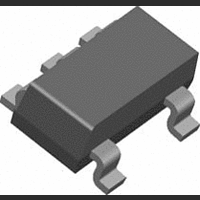
LP2985IM5-3.3 National Semiconductor, LP2985IM5-3.3 Datasheet - Page 6

LP2985IM5-3.3
Manufacturer Part Number
LP2985IM5-3.3
Description
Voltage Regulator IC
Manufacturer
National Semiconductor
Specifications of LP2985IM5-3.3
No. Of Pins
5
Output Current
0.15A
Mounting Type
Surface Mount
Voltage Regulator Type
LDO Linear
Peak Reflow Compatible (260 C)
No
Output Voltage
3.3V
Current Rating
150mA
Output Voltage Max
3.3V
Lead Free Status / RoHS Status
Contains lead / RoHS non-compliant
Available stocks
Company
Part Number
Manufacturer
Quantity
Price
Company:
Part Number:
LP2985IM5-3.3
Manufacturer:
NSC
Quantity:
524
Part Number:
LP2985IM5-3.3
Manufacturer:
TI/德州仪器
Quantity:
20 000
Company:
Part Number:
LP2985IM5-3.3/NOPB
Manufacturer:
National Semiconductor
Quantity:
24 748
Company:
Part Number:
LP2985IM5-3.3/NOPB
Manufacturer:
NS
Quantity:
2 332
Part Number:
LP2985IM5-3.3/NOPB
Manufacturer:
TI/德州仪器
Quantity:
20 000
www.national.com
I
I
O
O
Limits in standard typeface are for T
less otherwise specified: V
Electrical Characteristics
Note 1: “Absolute Maximum Ratings” indicate limits beyond which damage to the component may occur. Electrical specifications do not apply when operating the
device outside of its rated operating conditions.
Note 2: The ESD rating of pins 3 and 4 is 1 kV.
Note 3: The maximum allowable power dissipation is a function of the maximum junction temperature, T
the ambient temperature, T
Where the value of
lowable dissipation will cause excessive die temperature, and the regulator will go into thermal shutdown.
Note 4: If used in a dual-supply system where the regulator load is returned to a negative supply, the LP2985 output must be diode-clamped to ground.
Note 5: The output PNP structure contains a diode between the V
turn on this diode.
Note 6: Limits are 100% production tested at 25˚C. Limits over the operating temperature range are guaranteed through correlation using Statistical Quality Control
(SQC) methods. The limits are used to calculate National’s Average Outgoing Quality Level (AOQL).
Note 7: Dropout voltage is defined as the input to output differential at which the output voltage drops 100 mV below the value measured with a 1V differential.
Note 8: The ON/OFF input must be properly driven to prevent possible misoperation. For details, refer to Application Hints.
Note 9: The LP2985 has foldback current limiting which allows a high peak current when V
forced to ground (see Typical Performance Characteristics curves).
(SC)
(PK)
Symbol
Ripple Rejection
Short Circuit Current
Peak Output Current
J-A
for the SOT-23 package is 220˚C/W in a typical PC board mounting and the micro SMD package is 320˚C/W. Exceeding the maximum al-
Parameter
A
. The maximum allowable power dissipation at any ambient temperture is calculated using:
IN
= V
O
(NOM) + 1V, I
J
= 25˚C. and limits in boldface type apply over the full operating temperature range. Un-
f = 1 kHz, C
C
R
(Note 9)
V
OUT
OUT
L
= 0 (Steady State)
(Continued)
= 10 µF
V
L
Conditions
o
= 1 mA, C
(NOM) −5%
IN
BYPASS
to V
OUT
= 10 nF
IN
terminals that is normally reverse-biased. Reversing the polarity from V
= 1 µF, C
6
OUT
OUT
Typ
400
350
45
>
= 4.7 µF, V
0.5V, and then reduces the maximum output current as V
J
(MAX), the junction-to-ambient thermal resistance,
LP2985AI-X.X
Min
(Note 6)
ON/OFF
Max
= 2V.
Min
LP2985I-X.X
(Note 6)
Max
IN
to V
J-A
OUT
Units
OUT
mA
mA
, and
dB
will
is


