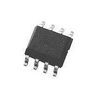
LMH6702MA National Semiconductor, LMH6702MA Datasheet - Page 11

LMH6702MA
Manufacturer Part Number
LMH6702MA
Description
Operational Amplifier (Op-Amp) IC
Manufacturer
National Semiconductor
Specifications of LMH6702MA
Op Amp Type
Low Distortion
No. Of Amplifiers
1
Bandwidth
720MHz
Slew Rate
3100V/µs
Supply Voltage Range
± 5V To ± 6V
Amplifier Case Style
SOIC
No. Of Pins
8
Number Of Channels
1
Common Mode Rejection Ratio (min)
45 dB
Input Offset Voltage
4.5 mV at +/- 5 V
Supply Current
16.1 mA at +/- 5 V
Maximum Operating Temperature
+ 85 C
Package / Case
SOIC-8 Narrow
Maximum Dual Supply Voltage
+/- 6 V
Minimum Operating Temperature
- 40 C
Lead Free Status / RoHS Status
Contains lead / RoHS non-compliant
Available stocks
Company
Part Number
Manufacturer
Quantity
Price
Part Number:
LMH6702MA
Manufacturer:
NS/国半
Quantity:
20 000
Part Number:
LMH6702MAX
Manufacturer:
NS/国半
Quantity:
20 000
Application Section
DC ACCURACY AND NOISE
Example below shows the output offset computation equa-
tion for the non-inverting configuration using the typical bias
current and offset specifications for A
Output Offset : V
Where R
inverting input.
Example computation for A
V
A good design, however, should include a worst case calcu-
lation using Min/Max numbers in the data sheet tables, in
order to ensure "worst case" operation.
Further improvement in the output offset voltage and drift is
possible using the composite amplifiers described in Appli-
cation Note OA-7. The two input bias currents are physically
unrelated in both magnitude and polarity for the current
feedback topology. It is not possible, therefore, to cancel
their effects by matching the source impedance for the two
inputs (as is commonly done for matched input bias current
devices).
The total output noise is computed in a similar fashion to the
output offset voltage. Using the input noise voltage and the
±
O
4.20mV
= (
±
6µA · 25Ω
IN
is the equivalent input impedance on the non-
O
= (
±
±
I
1mV) (1 + 237/237)
BN
· R
V
= +2, R
IN
±
V
IO
(Continued)
F
) (1 + R
V
= 237Ω, R
= + 2:
±
F
/R
8µA · 237 =
G
IN
)
±
= 25Ω:
I
BI
· R
F
11
two input noise currents, the output noise is developed
through the same gain equations for each term but com-
bined as the square root of the sum of squared contributing
elements. See Application Note OA-12 for a full discussion of
noise calculations for current feedback amplifiers.
PRINTED CIRCUIT LAYOUT
Generally, a good high frequency layout will keep power
supply and ground traces away from the inverting input and
output pins. Parasitic capacitances on these nodes to
ground will cause frequency response peaking and possible
circuit oscillations (see Application Note OA-15 for more
information). National Semiconductor suggests the following
evaluation boards as a guide for high frequency layout and
as an aid in device testing and characterization:
These free evaluation boards are shipped when a device
sample request is placed with National Semiconductor.
Device
LMH6702MF
LMH6702MA
Package
SOT23-5
SOIC
Evaluation Board
Part Number
CLC730216
CLC730227
www.national.com


