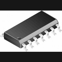
LMC6484AIM National Semiconductor, LMC6484AIM Datasheet - Page 12

LMC6484AIM
Manufacturer Part Number
LMC6484AIM
Description
Operational Amplifier (Op-Amp) IC
Manufacturer
National Semiconductor
Specifications of LMC6484AIM
No. Of Amplifiers
4
Slew Rate
1.3V/µs
No. Of Pins
14
Amplifier Type
Operational
Mounting Type
Surface Mount
Peak Reflow Compatible (260 C)
No
Leaded Process Compatible
No
Number Of Channels
4
Voltage Gain Db
116.47 dB
Common Mode Rejection Ratio (min)
70 dB
Input Offset Voltage
0.75 mV at 5 V
Operating Supply Voltage
5 V, 9 V, 12 V, 15 V
Supply Current
2.8 mA at 5 V
Maximum Operating Temperature
+ 85 C
Package / Case
SOIC-14 Narrow
Minimum Operating Temperature
- 40 C
Lead Free Status / RoHS Status
Contains lead / RoHS non-compliant
Available stocks
Company
Part Number
Manufacturer
Quantity
Price
Company:
Part Number:
LMC6484AIM
Manufacturer:
NS
Quantity:
8 004
Part Number:
LMC6484AIM
Manufacturer:
NS/国半
Quantity:
20 000
Part Number:
LMC6484AIM/NOPB
Manufacturer:
TI/德州仪器
Quantity:
20 000
Part Number:
LMC6484AIMX
Manufacturer:
NS/国半
Quantity:
20 000
www.national.com
Typical Performance Characteristics
specified (Continued)
Stability vs
Capacitive Load
Application Information
1.0 Amplifier Topology
The
wide-compliance range current mirrors and the body effect to
extend input common mode range to each supply rail.
Complementary paralleled differential input stages, like the
type used in other CMOS and bipolar rail-to-rail input ampli-
fiers, were not used because of their inherent accuracy prob-
lems due to CMRR, cross-over distortion, and open-loop
gain variation.
The LMC6484’s input stage design is complemented by an
output stage capable of rail-to-rail output swing even when
driving a large load. Rail-to-rail output swing is obtained by
taking the output directly from the internal integrator instead
of an output buffer stage.
2.0 Input Common-Mode Voltage Range
Unlike Bi-FET amplifier designs, the LMC6484 does not ex-
hibit phase inversion when an input voltage exceeds the
negative supply voltage. Figure 1 shows an input voltage ex-
ceeding both supplies with no resulting phase inversion on
the output.
The absolute maximum input voltage is 300 mV beyond ei-
ther supply rail at room temperature. Voltages greatly ex-
FIGURE 1. An Input Voltage Signal Exceeds the
LMC6484
LMC6484 Power Supply Voltages with
No Output Phase Inversion
incorporates
specially
DS011714-89
DS011714-10
designed
V
Stability vs
Capacitive Load
12
S
= +15V, Single Supply, T
ceeding this absolute maximum rating, as in Figure 2 , can
cause excessive current to flow in or out of the input pins
possibly affecting reliability.
Applications that exceed this rating must externally limit the
maximum input current to
shown in Figure 3 .
3.0 Rail-To-Rail Output
The approximated output resistance of the LMC6484 is
180
sourcing and 83
output resistance, maximum output voltage swing can be es-
timated as a function of load.
4.0 Capacitive Load Tolerance
The LMC6484 can typically directly drive a 100 pF load with
V
lower is the most sensitive configuration. Direct capacitive
S
= 15V at unity gain without oscillating. The unity gain fol-
Exceeds the 3V Supply in Figure 3 Causing
sourcing and 130
FIGURE 3. R
FIGURE 2. A
Voltages Exceeding the Supply Voltage
No Phase Inversion Due to R
sinking at V
I
Input Current Protection for
±
A
7.5V Input Signal Greatly
= 25˚C unless otherwise
±
sinking at V
5 mA with an input resistor as
S
= 5V. Using the calculated
DS011714-90
S
DS011714-11
= 3V and 110
I
DS011714-12


