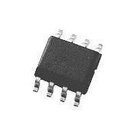
LMC6081AIM National Semiconductor, LMC6081AIM Datasheet - Page 8

LMC6081AIM
Manufacturer Part Number
LMC6081AIM
Description
Operational Amplifier (Op-Amp) IC
Manufacturer
National Semiconductor
Specifications of LMC6081AIM
No. Of Amplifiers
1
Slew Rate
1.5V/µs
No. Of Pins
8
Peak Reflow Compatible (260 C)
No
Leaded Process Compatible
No
Mounting Type
Surface Mount
Package / Case
8-NSOIC
Lead Free Status / RoHS Status
Contains lead / RoHS non-compliant
Available stocks
Company
Part Number
Manufacturer
Quantity
Price
Company:
Part Number:
LMC6081AIM
Manufacturer:
NS
Quantity:
960
Part Number:
LMC6081AIM
Manufacturer:
NS/国半
Quantity:
20 000
Part Number:
LMC6081AIMX
Manufacturer:
NS/国半
Quantity:
20 000
Company:
Part Number:
LMC6081AIMX/NOPB
Manufacturer:
MOT
Quantity:
6 220
Part Number:
LMC6081AIMX/NOPB
Manufacturer:
TI/德州仪器
Quantity:
20 000
www.national.com
Typical Performance Characteristics
specified (Continued)
Applications Hints
AMPLIFIER TOPOLOGY
The LMC6081 incorporates a novel op-amp design topology
that enables it to maintain rail-to-rail output swing even when
driving a large load. Instead of relying on a push-pull unity
gain output buffer stage, the output stage is taken directly
from the internal integrator, which provides both low output
impedance and large gain. Special feed-forward compensa-
tion design techniques are incorporated to maintain stability
over a wider range of operating conditions than traditional
micropower op-amps. These features make the LMC6081
both easier to design with, and provide higher speed than
products typically found in this ultra-low power class.
COMPENSATING FOR INPUT CAPACITANCE
It is quite common to use large values of feedback resis-
tance for amplifiers with ultra-low input current, like the
LMC6081.
Although the LMC6081 is highly stable over a wide range of
operating conditions, certain precautions must be met to
achieve the desired pulse response when a large feedback
resistor is used. Large feedback resistors and even small
values of input capacitance, due to transducers, photo-
diodes, and circuit board parasitics, reduce phase margins.
When high input impedances are demanded, guarding of the
LMC6081 is suggested. Guarding input lines will not only
reduce leakage, but lowers stray input capacitance as well.
(See Printed-Circuit-Board Layout for High Impedance
Work).
The effect of input capacitance can be compensated for by
adding a capacitor, C
Figure 1 ) such that:
or
Since it is often difficult to know the exact value of C
be experimentally adjusted so that the desired pulse re-
Stability vs Capacitive
f
, around the feedback resistors (as in
Load R
R
1
C
IN
≤ R
L
= 1 MΩ
2
C
f
01142335
IN
, C
f
can
V
8
S
=
sponse is achieved. Refer to the LMC660 and LMC662 for a
more detailed discussion on compensating for input capaci-
tance.
CAPACITIVE LOAD TOLERANCE
All rail-to-rail output swing operational amplifiers have volt-
age gain in the output stage. A compensation capacitor is
normally included in this integrator stage. The frequency
location of the dominant pole is affected by the resistive load
on the amplifier. Capacitive load driving capability can be
optimized by using an appropriate resistive load in parallel
with the capacitive load (see typical curves).
Direct capacitive loading will reduce the phase margin of
many op-amps. A pole in the feedback loop is created by the
combination of the op-amp’s output impedance and the ca-
pacitive load. This pole induces phase lag at the unity-gain
crossover frequency of the amplifier resulting in either an
oscillatory or underdamped pulse response. With a few ex-
ternal components, op amps can easily indirectly drive ca-
pacitive loads, as shown in Figure 2.
±
FIGURE 1. Cancelling the Effect of Input Capacitance
7.5V, T
A
= 25˚C, Unless otherwise
01142304


