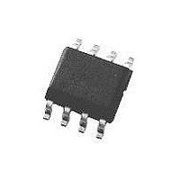
LMC6062AIM National Semiconductor, LMC6062AIM Datasheet - Page 8

LMC6062AIM
Manufacturer Part Number
LMC6062AIM
Description
Operational Amplifier (Op-Amp) IC
Manufacturer
National Semiconductor
Specifications of LMC6062AIM
No. Of Amplifiers
2
Slew Rate
0.035V/µs
No. Of Pins
8
Peak Reflow Compatible (260 C)
No
Leaded Process Compatible
No
Mounting Type
Surface Mount
Package / Case
8-NSOIC
Lead Free Status / RoHS Status
Contains lead / RoHS non-compliant
Available stocks
Company
Part Number
Manufacturer
Quantity
Price
Company:
Part Number:
LMC6062AIM
Manufacturer:
NS
Quantity:
120
www.national.com
Applications Hints
CAPACITIVE LOAD TOLERANCE
All rail-to-rail output swing operational amplifiers have volt-
age gain in the output stage. A compensation capacitor is
normally included in this integrator stage. The frequency lo-
cation of the dominate pole is affected by the resistive load
on the amplifier. Capacitive load driving capability can be op-
timized by using an appropriate resistive load in parallel with
the capacitive load (see typical curves).
Direct capacitive loading will reduce the phase margin of
many op-amps. A pole in the feedback loop is created by the
combination of the op-amp’s output impedance and the ca-
pacitive load. This pole induces phase lag at the unity-gain
crossover frequency of the amplifier resulting in either an os-
cillatory or underdamped pulse response. With a few exter-
nal components, op amps can easily indirectly drive capaci-
tive loads, as shown in Figure 2 .
In the circuit of Figure 2 , R1 and C1 serve to counteract the
loss of phase margin by feeding the high frequency compo-
nent of the output signal back to the amplifier’s inverting in-
put, thereby preserving phase margin in the overall feedback
loop.
Capacitive load driving capability is enhanced by using a pull
up resistor to V
ducting 10 µA or more will significantly improve capacitive
load responses. The value of the pull up resistor must be de-
termined based on the current sinking capability of the ampli-
FIGURE 2. LMC6062 Noninverting Gain of 10 Amplifier,
FIGURE 1. Canceling the Effect of Input Capacitance
Compensated to Handle Capacitive Loads
+
( Figure 3 ). Typically a pull up resistor con-
(Continued)
DS011298-5
DS011298-4
8
fier with respect to the desired output swing. Open loop gain
of the amplifier can also be affected by the pull up resistor
(see Electrical Characteristics).
PRINTED-CIRCUIT-BOARD LAYOUT
FOR HIGH-IMPEDANCE WORK
It is generally recognized that any circuit which must operate
with less than 1000 pA of leakage current requires special
layout of the PC board. When one wishes to take advantage
of the ultra-low bias current of the LMC6062, typically less
than 10 fA, it is essential to have an excellent layout. Fortu-
nately, the techniques of obtaining low leakages are quite
simple. First, the user must not ignore the surface leakage of
the PC board, even though it may sometimes appear accept-
ably low, because under conditions of high humidity or dust
or contamination, the surface leakage will be appreciable.
To minimize the effect of any surface leakage, lay out a ring
of foil completely surrounding the LMC6062’s inputs and the
terminals of capacitors, diodes, conductors, resistors, relay
terminals etc. connected to the op-amp’s inputs, as in Figure
4 . To have a significant effect, guard rings should be placed
on both the top and bottom of the PC board. This PC foil
must then be connected to a voltage which is at the same
voltage as the amplifier inputs, since no leakage current can
flow between two points at the same potential. For example,
a PC board trace-to-pad resistance of 10
mally considered a very large resistance, could leak 5 pA if
the trace were a 5V bus adjacent to the pad of the input. This
would cause a 100 times degradation from the LMC6062’s
actual performance. However, if a guard ring is held within
5 mV of the inputs, then even a resistance of 10
cause only 0.05 pA of leakage current. See Figure 5 for typi-
cal connections of guard rings for standard op-amp
configurations.
FIGURE 3. Compensating for Large Capacitive Loads
FIGURE 4. Example of Guard Ring in P.C. Board
with a Pull Up Resistor
Layout
DS011298-14
12
, which is nor-
11
DS011298-6
would


