LM8261M5 National Semiconductor, LM8261M5 Datasheet
LM8261M5
Specifications of LM8261M5
Available stocks


Related parts for LM8261M5

LM8261M5 Summary of contents
Page 1
... The output stage has low distortion (0.05% THD+N) and can supply a respectable amount of current (15mA) with minimal headroom from either rail (300mV). © 2000 National Semiconductor Corporation The LM8261 is offered in the space saving SOT23-5 pack- age. Features ...
Page 2
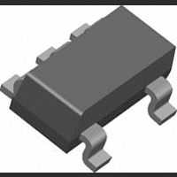
... Connection Diagram Ordering Information Package Ordering Info 5-Pin SOT-23 LM8261M5 LM8261M5X www.national.com SOT23-5 DS101084-62 Top View Pkg Marking Supplied AS 1K Units Tape and Reel A45A 3K Units Tape and Reel 2 NSC Drawing MA05B ...
Page 3
... Absolute Maximum Ratings If Military/Aerospace specified devices are required, please contact the National Semiconductor Sales Office/ Distributors for availability and specifications. ESD Tolerance V Differential IN Output Short Circuit Duration + − Supply Voltage ( Voltage at Input/Output pins Storage Temperature Range 2.7V Electrical Characteristics Unless otherwise specified, all limits guaranteed for T > ...
Page 4
Electrical Characteristics Unless otherwise specified, all limits guaranteed for T > − Boldface limits apply at the temperature extremes. L Symbol Parameter f Unity Gain-Frequency u GBWP Gain Bandwidth Product Phi Phase Margin m ...
Page 5
Electrical Characteristics Unless otherwise specified, all limited guaranteed for T > − Boldface limits apply at the temperature extremes. L Symbol Parameter I Supply Current S SR Slew Rate (Note 8) f Unity Gain ...
Page 6
Electrical Characteristics Unless otherwise specified, all limited guaranteed for T > 0V. Boldface limits apply at the temperature extremes. L Symbol Parameter A Large Signal Voltage Gain VOL V Output Swing O High Output Swing Low ...
Page 7
Typical Performance Characteristics V vs. V for 3 Representative Units vs. V for 3 Representative Units vs. V for 3 Representative Units 25˚C, Unless Otherwise Noted A V vs. V ...
Page 8
Typical Performance Characteristics www.national.com T = 25˚C, Unless Otherwise Noted (Continued vs DS101084- DS101084-27 I ...
Page 9
Typical Performance Characteristics I vs. V (NPN side Unity Gain Frequency vs Unity Gain Freq. and Phase Margin vs 25˚C, Unless Otherwise Noted (Continued) A Gain/Phase vs. Frequency DS101084-26 Phase Margin vs. V ...
Page 10
Typical Performance Characteristics Phase Margin vs. Load CMRR vs. Frequency −PSRR vs. Frequency www.national.com T = 25˚C, Unless Otherwise Noted (Continued) A Unity Gain Freq. and Phase Margin vs. C DS101084-6 +PSRR vs. Frequency DS101084-14 Output Voltage vs. Output Sourcing ...
Page 11
Typical Performance Characteristics Output Voltage vs. Output Sourcing Current Max Output Swing vs. Load % Overshoot vs. Cap Load T = 25˚C, Unless Otherwise Noted (Continued) A Output Voltage vs. Output Sinking Current DS101084-44 Max Output Swing vs. Frequency DS101084-10 ...
Page 12
Typical Performance Characteristics +SR vs. Cap Load +SR vs. Cap Load Settling Time vs. Error Voltage www.national.com T = 25˚C, Unless Otherwise Noted (Continued) A −SR vs. Cap Load DS101084-51 −SR vs. Cap Load DS101084-49 Settling Time vs. Error Voltage ...
Page 13
Typical Performance Characteristics Input Noise Voltage/Current vs. Frequency Input Noise Current for Various V CM Input Noise Current vs 25˚C, Unless Otherwise Noted (Continued) A Input Noise Voltage for Various V DS101084-15 Input Noise Voltage vs. ...
Page 14
Typical Performance Characteristics THD+N vs. Frequency THD+N vs. Amplitude Small Signal Step Response www.national.com T = 25˚C, Unless Otherwise Noted (Continued) A THD+N vs. Frequency DS101084-22 THD+N vs. Amplitude DS101084-19 Large Signal Step Response DS101084-38 14 DS101084-21 DS101084-20 DS101084-40 ...
Page 15
Application Notes: Block Diagram and Operational Description: A) Input Stage: As can be seen from the simplified schematic in Figure 1 , the input stage consists of two distinct differential pairs (Q1-Q2 and Q3-Q4) in order to accommodate the full ...
Page 16
Application Notes: (Continued) Op Amp’s compensation capacitor value and available cur- rent into that capacitor. Beyond 10nF, the Slew Rate is deter- mined by the Op Amp’s available output current. Note that because of the lower output sourcing current compared ...
Page 17
Application Notes: (Continued) FIGURE 7. Output Sinking Characteristics with Load Lines TFT applications: Figure 8 below, shows a typical application where the LM8261 is used as a buffer amplifier for the V ployed in a TFT LCD flat panel: FIGURE ...
Page 18
Application Notes: (Continued) Other Application Hints: The use of supply decoupling is mandatory in most applica- tions. As with most relatively high speed/high output current Op Amps, best results are achieved when each supply line is decoupled with two capacitors; ...
Page 19
... NATIONAL’S PRODUCTS ARE NOT AUTHORIZED FOR USE AS CRITICAL COMPONENTS IN LIFE SUPPORT DEVICES OR SYSTEMS WITHOUT THE EXPRESS WRITTEN APPROVAL OF THE PRESIDENT AND GENERAL COUNSEL OF NATIONAL SEMICONDUCTOR CORPORATION. As used herein: 1. Life support devices or systems are devices or systems which, (a) are intended for surgical implant ...