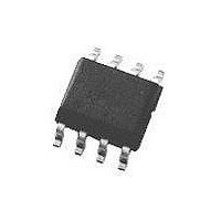
LM7372MR National Semiconductor, LM7372MR Datasheet - Page 5

LM7372MR
Manufacturer Part Number
LM7372MR
Description
Operational Amplifier (Op-Amp) IC
Manufacturer
National Semiconductor
Specifications of LM7372MR
Op Amp Type
High Speed
No. Of Amplifiers
2
Slew Rate
3000V/µs
No. Of Pins
8
Operating Temperature Range
-40°C To +85°C
Termination Type
SMD
Amplifier Type
Operational
Lead Free Status / RoHS Status
Contains lead / RoHS non-compliant
Available stocks
Company
Part Number
Manufacturer
Quantity
Price
Company:
Part Number:
LM7372MR
Manufacturer:
nstion
Quantity:
210
Part Number:
LM7372MR
Manufacturer:
NS/国半
Quantity:
20 000
V
I
I
SR
φ
t
t
A
φ
hd2
hd3
e
i
SC
S
n
S
P
Symbol
Symbol
m
D
n
O
D
±
Unless otherwise specified, all limits guaranteed for T
extremes.
Unless otherwise specified, all limits guaranteed for T
extremes.
Note 1: Absolute Maximum Ratings indicate limits beyond which damage to the device may occur. Operating Ratings indicate conditions for which the device is
intended to be functional, but specific performance is not guaranteed. For guaranteed specifications and the test conditions, see the Electrical Characteristics.
Note 2: For testing purposes, ESD was applied using human body model, 1.5kΩ in series with 100pF. Machine model, 0Ω in series with 200pF.
Note 3: Applies to both single-supply and split-supply operation. Continuous short circuit operation at elevated ambient temperature can result in exceeding the
maximum allowed junction temperature of 150˚C.
Note 4: The maximum power dissipation is a function of T
(T
4sq. in of 1oz CU connected to pins 1,6,8,9 & 16, θ
Note 5: Typical values represent the most likely parametic norm.
Note 6: All limits are guaranteed by testing or statistical analysis.
Note 7: Large signal voltage gain is the total output swing divided by the input signal required to produce that swing. For V
V
Note 8: Slew Rate is the average of the rising and falling slew rates.
Note 9: Differential gain and phase are measured with A
±
OUT
(JMAX)
5V DC Electrical Characteristics
5V AC Electrical Characteristics
=
±
– T
2V
A
Output Swing
Output Short Circuit Current
Supply Current (both Amps)
Slew Rate (Note 8)
Unity Bandwidth Product
−3dB Frequency
Phase Margin
Settling Time (0.1%)
Propagation Delay
Differential Gain (Note 9)
Differential Phase (Note 9)
Second Harmonic Distortion
F
Third Harmonic Distortion
F
Input-Referred Voltage Noise
Input-Referred Current Noise
)/θ
IN
IN
JA
= 1MHz, A
= 1MHz, A
. All numbers apply for packages soldered directly into a PC board. The value for θ
Parameter
V
V
Parameter
= +2
= +2
JA
for the SOIC 16 is decreased to 70˚C/W.
V
= +2, V
(JMAX)
, θ
R
I
I
Sourcing
Sinking
OUT
OUT
IN
L
A
A
A
500Ω
A
500Ω
V
V
f = 10kHz
f = 10kHz
J
J
JA
= 1V
V
V
V
V
OUT
OUT
= 1kΩ
= 25˚C, V
= 25˚C, V
, and T
= +2, V
= +2
= −1, V
= +2, V
= − 80mA
= 80mA
(Continued)
PP
= 2V
= 2V
Conditions
at 3.58 MHz and output is 150Ω terminated.
A
. The maximum allowable power dissipation at any ambient temperature is P
5
Conditions
P-P
P-P
IN
O
IN
CM
CM
=
3V
=
, R
, R
= 0V and R
= 0V and R
±
±
P-P
L
L
1V, R
1V, R
= 100Ω
= 100Ω
L
L
=
=
JA
L
L
is 106˚C/W for the SOIC 16 package. With a total area of
= 1kΩ. Boldface apply at the temperature
= 1kΩ. Boldface apply at the temperature
(Note 6)
−3.2
−3.0
−2.5
−2.2
Min
(Note 6)
3.2
3.0
2.5
2.2
Min
S
(Note 5)
=
(Note 5)
−3.4
−2.7
±
12.4
Typ
150
150
3.4
2.8
15V, V
0.02
0.03
Typ
700
100
125
−84
−94
1.8
70
70
14
7
OUT
=
(Note 6)
(Note 6)
±
Max
Max
16
18
10V. For V
www.national.com
S
nV/
pA/
Units
Units
=
MHz
MHz
V/µs
deg
deg
dBc
dBc
mA
mA
mA
ns
ns
%
±
V
V
V
V
D
5V,
=


