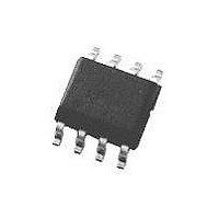
LM6181IM-8 National Semiconductor, LM6181IM-8 Datasheet - Page 21

LM6181IM-8
Manufacturer Part Number
LM6181IM-8
Description
Operational Amplifier (Op-Amp) IC
Manufacturer
National Semiconductor
Specifications of LM6181IM-8
No. Of Amplifiers
1
Bandwidth
100MHz
No. Of Pins
8
Peak Reflow Compatible (260 C)
No
Leaded Process Compatible
No
Mounting Type
Surface Mount
Package / Case
8-NSOIC
Number Of Channels
1
Common Mode Rejection Ratio (min)
50 dB
Input Offset Voltage
3 mV at +/- 5 V
Operating Supply Voltage
9 V, 12 V, 15 V, 18 V, 24 V, 28 V
Supply Current
8.5 mA at +/- 5 V
Maximum Operating Temperature
+ 85 C
Maximum Dual Supply Voltage
+/- 16 V
Minimum Operating Temperature
- 40 C
Lead Free Status / RoHS Status
Contains lead / RoHS non-compliant
Available stocks
Company
Part Number
Manufacturer
Quantity
Price
Company:
Part Number:
LM6181IM-8
Manufacturer:
NS
Quantity:
345
Part Number:
LM6181IM-8
Manufacturer:
NS/国半
Quantity:
20 000
Company:
Part Number:
LM6181IM-8/NOPB
Manufacturer:
TI
Quantity:
25
Typical Applications
CURRENT FEEDBACK TOPOLOGY
For a conventional voltage feedback amplifier the resulting
small-signal bandwidth is inversely proportional to the de-
sired gain to a first order approximation based on the gain-
bandwidth concept. In contrast, the current feedback ampli-
fier topology, such as the LM6181, transcends this limitation
to offer a signal bandwidth that is relatively independent of
the closed-loop gain. Figure 1a and Figure 1b illustrate that
for closed loop gains of −1 and −5 the resulting pulse fidelity
suggests quite similar bandwidths for both configurations.
The closed-loop bandwidth of the LM6181 depends on the
feedback resistance, R
varied to adjust for the desired closed-loop gain as in Figure
2.
FIGURE 1. 1a, 1b: Variation of Closed Loop Gain
from −1 to −5 Yields Similar Responses
f
. Therefore, R
1a
1b
S
and not R
f
, must be
01132812
01132813
21
POWER SUPPLY BYPASSING AND LAYOUT
CONSIDERATIONS
A fundamental requirement for high-speed amplifier design
is adequate bypassing of the power supply. It is critical to
maintain a wideband low-impedance to ground at the ampli-
fiers supply pins to insure the fidelity of high speed amplifier
transient signals. 10 µF tantalum and 0.1 µF ceramic bypass
capacitors are recommended for each supply pin. The by-
pass capacitors should be placed as close to the amplifier
pins as possible (0.5" or less).
FEEDBACK RESISTOR SELECTION: R
Selecting the feedback resistor, R
compensating the LM6181. For general applications the
LM6181 will maintain specified performance with an 820Ω
feedback resistor. Although this value will provide good re-
sults for most applications, it may be advantageous to adjust
this value slightly. Consider, for instance, the effect on pulse
responses with two different configurations where both the
closed-loop gains are 2 and the feedback resistors are 820Ω
and 1640Ω, respectively. Figure 3a and Figure 3b illustrate
the effect of increasing R
closed-loop gain — the amplifier bandwidth decreases. Ac-
cordingly, larger feedback resistors can be used to slow
down the LM6181 (see −3 dB bandwidth vs R
and reduce overshoot in the time domain response. Con-
versely, smaller feedback resistance values than 820Ω can
be used to compensate for the reduction of bandwidth at
high closed loop gains, due to 2nd order effects. For ex-
ample Figure 4 illustrates reducing R
the desired small signal response in an amplifier configured
for a closed loop gain of 25.
the Desired Closed Loop Gain, A
FIGURE 2. R
S
Is Adjusted to Obtain
f
while maintaining the same
f
, is a dominant factor in
f
01132814
to 500Ω to establish
f
f
typical curves)
VCL
www.national.com


