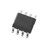
LM5104M National Semiconductor, LM5104M Datasheet - Page 4

LM5104M
Manufacturer Part Number
LM5104M
Description
MOSFET Driver IC
Manufacturer
National Semiconductor
Specifications of LM5104M
Driver Case Style
NSOIC
No. Of Pins
8
Peak Reflow Compatible (260 C)
No
Leaded Process Compatible
No
Package / Case
8-NSOIC
Lead Free Status / RoHS Status
Contains lead / RoHS non-compliant
Available stocks
Company
Part Number
Manufacturer
Quantity
Price
Part Number:
LM5104M
Manufacturer:
NS/国半
Quantity:
20 000
Part Number:
LM5104M/NOPB
Manufacturer:
NS/国半
Quantity:
20 000
www.national.com
V
I
I
THERMAL RESISTANCE
θ
t
t
t
t
t
OHH
OLH
LPHL
HPHL
RC
R
BS
JA
Electrical Characteristics
apply over the full operating junction temperature range. Unless otherwise specified, V
RT = 100kΩ. No Load on LO or HO. (Continued)
OHH
Switching Characteristics
type apply over the full operating junction temperature range. Unless otherwise specified, V
0V, No Load on LO or HO .
, t
Note 1: Absolute Maximum Ratings indicate limits beyond which damage to the component may occur. Operating Ratings are conditions under which operation of
the device is guaranteed. Operating Ratings do not imply guaranteed performance limits. For guaranteed performance limits and associated test conditions, see the
Electrical Characteristics tables.
Note 2: The human body model is a 100 pF capacitor discharged through a 1.5kΩ resistor into each pin. 2 kV for all pins except Pin 2, Pin 3 and Pin 4 which are
rated at 500V.
Note 3: 4 layer board with Cu finished thickness 1.5/1/1/1.5 oz. Maximum die size used. 5x body length of Cu trace on PCB top. 50 x 50mm ground and power
planes embedded in PCB. See Application Note AN-1187.
Note 4: Min and Max limits are 100% production tested at 25˚C. Limits over the operating temperature range are guaranteed through correlation using Statistical
Quality Control (SQC) methods. Limits are used to calculate National’s Average Outgoing Quality Level (AOQL).
Note 5: The θ
Symbol
Symbol
, t
F
FC
JA
High-Level Output Voltage
Peak Pullup Current
Peak Pulldown Current
Junction to Ambient
Lower Turn-Off Propagation Delay (IN
Rising to LO Falling)
Upper Turn-Off Propagation Delay (IN
Falling to HO Falling)
Either Output Rise/Fall Time
Either Output Rise/Fall Time
(3V to 9V)
Bootstrap Diode Turn-Off Time
is not a given constant for the package and depends on the printed circuit board design and the operating environment.
Parameter
Parameter
Specifications in standard typeface are for T
Specifications in standard typeface are for T
I
V
V
V
SOIC-8
LLP-10 (Note 3)
C
C
I
HO
F
OHH
HO
HO
L
L
= 20 mA, I
= 1000 pF
= 0.1 µF
= –100 mA,
= 0V
= 12V
4
= V
Conditions
Conditions
HB
– V
R
= 200 mA
HO
J
= +25˚C, and those in boldface type
DD
Min
Min
J
= +25˚C, and those in boldface
= V
DD
HB
= V
= 12V, V
0.35
Typ
Typ
170
1.6
1.8
0.6
40
25
25
15
50
HB
= 12V, V
SS
Max
0.55
Max
= V
56
56
SS
HS
= V
= 0V,
HS
Units
Units
˚C/W
ns
ns
ns
µs
ns
V
A
A
=


